
Homework Answers

Add Answer to:
. Ratioed Logic, 25pts Consider a 4-input NOR gate implemented in pseudo-NMOS logic driving an in...
a) What is the logic function implemented by the gate on the right? b) Design the...
 a) What is the logic function implemented by the gate on the right? b) Design the NMOS transistor network and select the device sizes for the PMOS and NMOS transistors to give a delay similar to that of the typical symmetric CMOS reference inverter (W/L-12/1,5/1]) with the same C. c) What is the equivalent W/L ratio of the PMOS switching network then all of the PMOS transistors are on? SV D Logic inputs .toF NMOS network
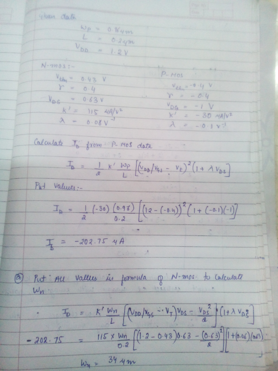
Compute the following for the pseudo-NMOS inverter shown in Figure. VTn=0.45V. VTp=. 0.45V kn-115uA/V2.kp'--304A/V2, VDSATn=0.4V, VDSATp=...
 Compute the following for the pseudo-NMOS inverter shown in Figure. VTn=0.45V. VTp=. 0.45V kn-115uA/V2.kp'--304A/V2, VDSATn=0.4V, VDSATp= -0.4V. Transistors are short channel devices. a. VOL and VOH b. Which is expected to have a higher value? NML or NMH? Why? c. Why is the circuit called a pseudo-NMOS inverter? d. The power dissipation: (1) for Vin low, and (2) for Vin high. Output load is 1 pF e. For an output load of 1 pF, calculate tpLH and tpHL. Are the...
CMOS Design Styles Quiz Problem 1: a) What is the typical "topology" for pMOS and nMOS...
CMOS Design Styles Quiz Problem 1: a) What is the typical "topology" for pMOS and nMOS in digital circuitry? -pMOS Vdd to Vout, nMOS Vout to Gnd -nMOS Vdd to Vout, pMOS Vout to Gnd -pMOS Vdd to Gnd, nMOS Vin to Vout -Only use xMOS -Both transistors Vin to Vout b) How do you implement nMOS in AND functions? -series connected, with increased widths -Parallel connected, with standard widths -Series connected with half the widths -Parallel connected, alternating large...
1. Consider the circuit below a. What is the logic function implemented by the CMOS transistor...
 1. Consider the circuit below a. What is the logic function implemented by the CMOS transistor network? Size the NMOS and PMOS devices so that the output resistance is the same as that of an inverter with an NMOS WIL 4 and PMOS W/L 8 b. What are the input patterns that give the worst case tpHL and tpLH. State clearly what are the initial input patterns and which input(s) has to make a transition in order to achieve this...
 a) What is the logic function implemented by the gate on the right? b) Design the NMOS transistor network and select the device sizes for the PMOS and NMOS transistors to give a delay similar to that of the typical symmetric CMOS reference inverter (W/L-12/1,5/1]) with the same C. c) What is the equivalent W/L ratio of the PMOS switching network then all of the PMOS transistors are on? SV D Logic inputs .toF NMOS network
 Compute the following for the pseudo-NMOS inverter shown in Figure. VTn=0.45V. VTp=. 0.45V kn-115uA/V2.kp'--304A/V2, VDSATn=0.4V, VDSATp= -0.4V. Transistors are short channel devices. a. VOL and VOH b. Which is expected to have a higher value? NML or NMH? Why? c. Why is the circuit called a pseudo-NMOS inverter? d. The power dissipation: (1) for Vin low, and (2) for Vin high. Output load is 1 pF e. For an output load of 1 pF, calculate tpLH and tpHL. Are the...
 1. Consider the circuit below a. What is the logic function implemented by the CMOS transistor network? Size the NMOS and PMOS devices so that the output resistance is the same as that of an inverter with an NMOS WIL 4 and PMOS W/L 8 b. What are the input patterns that give the worst case tpHL and tpLH. State clearly what are the initial input patterns and which input(s) has to make a transition in order to achieve this...
Most questions answered within 3 hours.
-
Write an assessment of the current business analysis of Hilton
Worldwide using Porters 5 Forces analysis.
asked 3 seconds from now -
i need help on this
Chapter 9 Section 3 Question 1:
Rudy puts this poster, with...
asked 8 minutes ago -
True or false Assembly x86
41. _____ The program counter is a pointer to the
instruction....
asked 9 minutes ago -
You have conducted an experiment to try to demonstrate that
growth factor receptor X protein (GFRX)...
asked 24 minutes ago -
The Gross Profit ratio for 2014 is 57.07%
Assume that Campbell's net sales for the first...
asked 24 minutes ago -
Thoroughly discuss the various current and proposed solutions to
anthropogenic influences resulting in Global Climate Change....
asked 28 minutes ago -
BLOG EXERCISE: You are writing a weekly intranet blog for the
CEO of a large Canadian...
asked 31 minutes ago -
calculate ΔGrxn at 36 ∘C. N2O4(g)→2NO2(g)
asked 31 minutes ago -
Present and Future Values of Single Cash Flows for Different
Periods
Find the following values, using...
asked 34 minutes ago -
Which types of mutations in DNA can lead to the translation of a
non-functional protein product?...
asked 33 minutes ago -
Many structures are composed of individual elements that react
in unison when forces are applied. the...
asked 34 minutes ago -
Work of 1950 J is done by stirring a perfectly insulated beaker
containing 75 g of...
asked 1 hour ago