
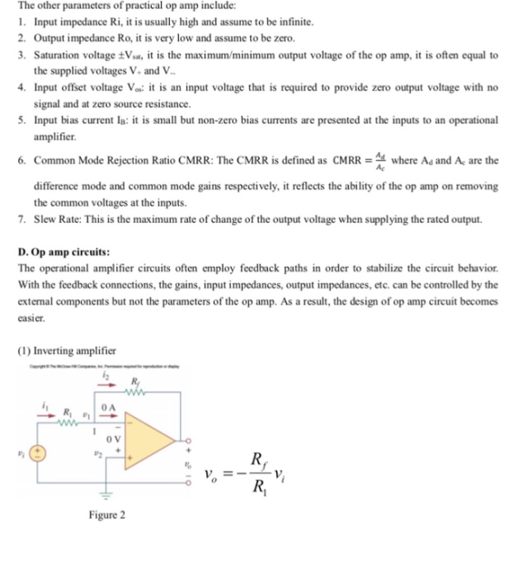
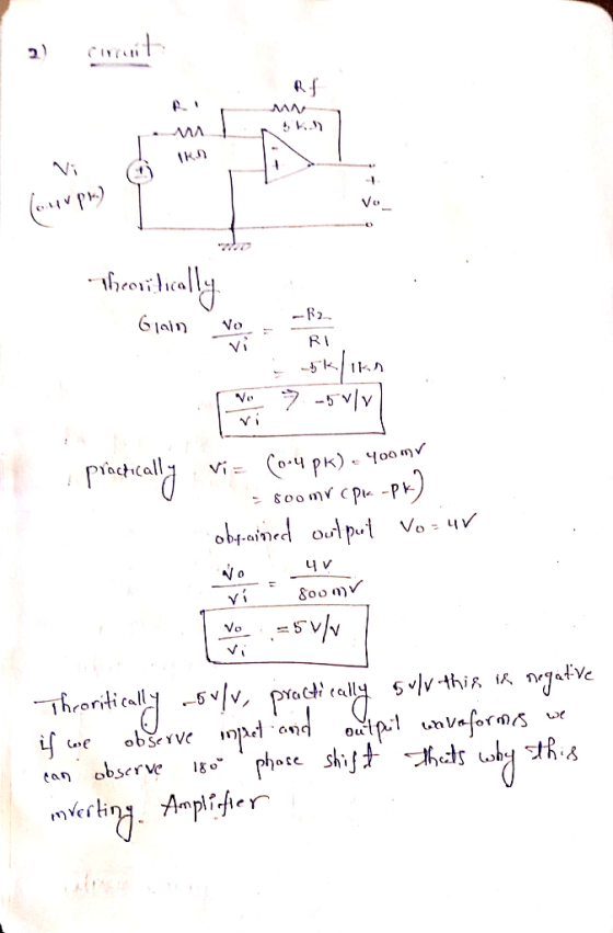
The other parameters of practical op amp include: . Input impedance Ri, is usually high and assume to be infinite 2. Output impedance Ro, it is very low and assume to be zero. 3. Saturation voltage V,t is the maximum/minimum output voltage of the op amp, i is often equal to the supplied voltages V and V signal and at zero source resistance amplifier 4. Input offset voltage Vos: it is an input voltage that is required to provide zero output voltage with no 5. Input bias current I:it is small but non-zero bias currents are presented at the inputs to an operational 6, Common Mode Rejection Ratio CMRR: The CMRR is defined as CMRR Ad where Ad and A are the difference mode and common mode gains respectively, it reflects the ability of the op amp on removing the common voltages at the inputs 7. Slew Rate: This is the maximum rate of change of the output voltage when supplying the rated output. D. Op amp circuits: The operational amplifier circuits often employ feedback paths in order to stabilize the circuit behavior. With the feedback connections, the gains, input impedances, output impedances, etc. can be controlled by the external components but not the parameters of the op amp. As a result, the design of op amp circuit becomes easier (1) Inverting amplifier O A 0 V Figure 2
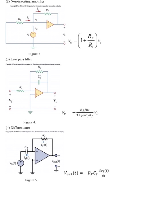
(2) Non-inverting amplifier Figure 3 (3) Low pass filter Rf/Ri 0 1+jaCR Figure 4 4) Differentiator RF iF(t) istt) ourlt) Vstt) Vout (tREC s() dt Figure 5
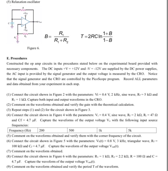
(5) Relaxation oscillator R, +R Figure 6. E. Procedures Constructed the op amp circuits in the procedures stated below on the experimental board provided with necessary components. The DC inputs +V- +12V and-V--12V are supplied by the DC power supplies, the AC input is provided by the signal generator and the output voltage is measured by the CRO. Notice that the signal generator and the CRO are controlled by the PicoScope program. Record ALL parameters and data obtained from your experiment in each step (1) Connect the circuit shown in Figure 2 with the parameters: Vi 0.4 V, 2 kHz, sine wave, Rf-5 kΩ and Ri -1 k2. Capture both input and output waveforms in the CRO (2) Comment on the waveforms obtained and verify the gain with the theoretical calculation. (3) Repeat steps (1) and (2) for the circuit shown in Figure 3 (4) Connect the circuit shown in Figure 4 with the parameters: V,-0.4 V, sine wave, Rf 2 kQ, R. 47 Ω and C-47 μF, Capture the waveforms of the output voltage Vo with the following input source frequencies: Frequency (Hz) 200 (5) Comment on the waveforms obtained and verify them with the corner frequency of the circuit. (6) Connect the circuit shown in Figure 5 with the parameters: Vs(t) 0.8 V, 3 kHz, triangular wave, Rr 500 lk 5k 100 kS2 and Cr-4.7 F. Capture the waveform of the output voltage Vour(t) (7) Comment on the waveform obtained. (8) Connect the circuit shown in Figure 6 with the parameters: R,-1kQ, R2 2.2 kS2, R-100 Ω and C- 4.7 μF. Capture the waveform of the output voltage Vout(t). (9) Comment on the waveform obtained and verify the period T of the waveform.
Homework Answers


Add Answer to:
Laboratory 1: operation amplifier characteristics A. Objectives: 1. To study the basic characteri...
Laboratory 2: Transistor circuit characteristics A. Objectives: 1. To study the basic characteris...
 Laboratory 2: Transistor circuit characteristics A. Objectives: 1. To study the basic characteristics of a transistor circuit. 2. To study the bias circuit of a transistor circuit. B. Apparatus: 1. DC Power supply 2. Experimental boards and corresponding components 3. Electronic calculator (prepared by students) 4. Digital camera (prepared by students for photo taking of the experimental results) 5. Laptop computer with the software PicoScope 6 and Microsoft Word installed. 6. PicoScope PC Oscilloscope and its accessories. 7. Digital multi-meter....
c) In estimating DC imperfections (input offset voltage, input offset current and the inverting amplifier with...
 c) In estimating DC imperfections (input offset voltage, input offset current and the inverting amplifier with nominal gain of -100 using 1 current) of an op-map, an and 10MQ resistors is implemented using the op-amp as shown in Fig 2(a) below R2 10MQ R 100k Vi Vo Figure 2(a): Inverting amplifier Measurements are conducted on the output voltage of the inverting amplifier under the following conditions: (i) the input (V) is open circuited and the output voltage is found to...
Inverting Amplifier Figure 4.2 shows the fundamental configuration of Op-Amp in which it is used as...
 Inverting Amplifier Figure 4.2 shows the fundamental configuration of Op-Amp in which it is used as an inverting amplifier. In this configuration the ratio, R2/R1 completely controls the effective gain of the amplifier and it can be verified that the output voltage is equal to Vo = - (R2/R1)Vin R2 100K Q-10V R1 Vinow 20K 1 2 7 V Vo 3 -10v Figure 4.2 Part 1 - Inverting Amp: Procedure 1. Construct the circuit of figure 4.2 using Op-Amp IC...
2. Consider this non-inverting op-amp amplifier This non-inverting amplifier circuit uses an operational amplifier as a...
 2. Consider this non-inverting op-amp amplifier This non-inverting amplifier circuit uses an operational amplifier as a building block. Do around. The op-amp's gain is a "little a"), but the overall amplifier's gain is A Cbig A. Derive the value of the output voltage, ve, as a function of the input voltage not confuse the non-inverting amplifier with the operational amplifier that it is built a. and the op-amp's gain a. What is the overall amplifier's gain Avo/v? (20pts) b. We...
Part I: Inverting Amplifier Procedure: 1. Build the circuit model for inverting amplifier in PSpice with...
 Part I: Inverting Amplifier Procedure: 1. Build the circuit model for inverting amplifier in PSpice with the following parameters: Ri = 5 k 2, R2 = 20 ks2, V+ = 10 V, V-=-10 V. 2. Hand calculates the theoretical closed loop gain Vout/Vin of the circuit model. 3. Generate a triangular waveform for Vin with the amplitude of 1 V and the period of 1 ms. 4. Run simulation. a. Set circuit model parameters. i.e., for voltage source: click VPWL...
2. Design a non-inverting op-amp circuit with two resistors under the following conditions: a. The gain of the ampl...
 2. Design a non-inverting op-amp circuit with two resistors under the following conditions: a. The gain of the amplifier must be +10 b. The input range is ± 2V c. The total power consumed by the resistors must be less than 100 mW Show all the calculations required to design the amplifier circuit with the shown specifications.in details Use MULTISIM to create the op-amp circuit and print a fully labelled diagram of the circuits with the voltmeters displays showing both...
3- OPERATIONAL-AMPLIFIER Nominating ampliar Voltage Show OW Difference ampliar Wate Date amplizier Close R Vout Voutin...
 3- OPERATIONAL-AMPLIFIER Nominating ampliar Voltage Show OW Difference ampliar Wate Date amplizier Close R Vout Voutin Vout = vin Buffer = Inverting amplifier Dout = (1 + .. Vout V out 1 V2 ERR Vour (, - v3) Differential Amplifier Non-Inverting amplifier 1- Refer to the op amp in Fig. If v; = 0.5 V, calculate: (a) the output voltage Vos (b) the current in the 10-k! resistor. 25k92 10k02 Oo + 6 2. A 741 op amp has an...
1) Explain briefly about the differential amplifier with a neat diagram. (2Marks) ii) Consider the summing...
 1) Explain briefly about the differential amplifier with a neat diagram. (2Marks) ii) Consider the summing operational amplifier shown below. The resistances on the inputs are both 50 k12, and the feedback resistance is also 50 k12. If the input signal voltages are 66 mV and -85 mV, determine the output voltage, (2 Marks) R = 502 Roy - 50 kn R250 kn O V-66 m peak V-85 mV peak V. Output voltage ii) The input resistance of an inverting...
8.) In the OP amp circuit shown in Figure 8 , determine the value of resistor...
 8.) In the OP amp circuit shown in Figure 8 , determine the
value of resistor R2 needed to establish an input trip point
voltage of 6.75 Volts ( i.e. when input signal voltage V in exceeds
6.75 V the OP amp’s output voltage changes state ) . ( 60 pts )
R2 = _______________
If the OP AMP in Figure 8 was biased by DC voltages of + / - 15
Volts , and the value of resistor R2...
8.) In the OP amp circuit shown in Figure 8 , determine the
value of resistor R2 needed to establish an input trip point
voltage of 6.75 Volts ( i.e. when input signal voltage V in exceeds
6.75 V the OP amp’s output voltage changes state ) . ( 60 pts )
R2 = _______________
If the OP AMP in Figure 8 was biased by DC voltages of + / - 15
Volts , and the value of resistor R2...
(5pts) 11. A 0.5V peak-to-peak 1kHz sine wave with a 100mV DC offset is provided as...
 (5pts) 11. A 0.5V peak-to-peak 1kHz sine wave with a 100mV DC offset is provided as the input into a non- inverting operational amplifier with a gain of 20. If the output of the op-amp is read using an oscilloscope with AC coupling, then the value is close to a. 2V DC b. 2V peak-to-peak 1kHz sine wave c. 10V peak-to-peak 1kHz sine wave with 2V DC offset d. 10V peak-to-peak 1kHz sine wave only (5pts) 12. Which of the...
 Laboratory 2: Transistor circuit characteristics A. Objectives: 1. To study the basic characteristics of a transistor circuit. 2. To study the bias circuit of a transistor circuit. B. Apparatus: 1. DC Power supply 2. Experimental boards and corresponding components 3. Electronic calculator (prepared by students) 4. Digital camera (prepared by students for photo taking of the experimental results) 5. Laptop computer with the software PicoScope 6 and Microsoft Word installed. 6. PicoScope PC Oscilloscope and its accessories. 7. Digital multi-meter....
 c) In estimating DC imperfections (input offset voltage, input offset current and the inverting amplifier with nominal gain of -100 using 1 current) of an op-map, an and 10MQ resistors is implemented using the op-amp as shown in Fig 2(a) below R2 10MQ R 100k Vi Vo Figure 2(a): Inverting amplifier Measurements are conducted on the output voltage of the inverting amplifier under the following conditions: (i) the input (V) is open circuited and the output voltage is found to...
 Inverting Amplifier Figure 4.2 shows the fundamental configuration of Op-Amp in which it is used as an inverting amplifier. In this configuration the ratio, R2/R1 completely controls the effective gain of the amplifier and it can be verified that the output voltage is equal to Vo = - (R2/R1)Vin R2 100K Q-10V R1 Vinow 20K 1 2 7 V Vo 3 -10v Figure 4.2 Part 1 - Inverting Amp: Procedure 1. Construct the circuit of figure 4.2 using Op-Amp IC...
 2. Consider this non-inverting op-amp amplifier This non-inverting amplifier circuit uses an operational amplifier as a building block. Do around. The op-amp's gain is a "little a"), but the overall amplifier's gain is A Cbig A. Derive the value of the output voltage, ve, as a function of the input voltage not confuse the non-inverting amplifier with the operational amplifier that it is built a. and the op-amp's gain a. What is the overall amplifier's gain Avo/v? (20pts) b. We...
 Part I: Inverting Amplifier Procedure: 1. Build the circuit model for inverting amplifier in PSpice with the following parameters: Ri = 5 k 2, R2 = 20 ks2, V+ = 10 V, V-=-10 V. 2. Hand calculates the theoretical closed loop gain Vout/Vin of the circuit model. 3. Generate a triangular waveform for Vin with the amplitude of 1 V and the period of 1 ms. 4. Run simulation. a. Set circuit model parameters. i.e., for voltage source: click VPWL...
 2. Design a non-inverting op-amp circuit with two resistors under the following conditions: a. The gain of the amplifier must be +10 b. The input range is ± 2V c. The total power consumed by the resistors must be less than 100 mW Show all the calculations required to design the amplifier circuit with the shown specifications.in details Use MULTISIM to create the op-amp circuit and print a fully labelled diagram of the circuits with the voltmeters displays showing both...
 3- OPERATIONAL-AMPLIFIER Nominating ampliar Voltage Show OW Difference ampliar Wate Date amplizier Close R Vout Voutin Vout = vin Buffer = Inverting amplifier Dout = (1 + .. Vout V out 1 V2 ERR Vour (, - v3) Differential Amplifier Non-Inverting amplifier 1- Refer to the op amp in Fig. If v; = 0.5 V, calculate: (a) the output voltage Vos (b) the current in the 10-k! resistor. 25k92 10k02 Oo + 6 2. A 741 op amp has an...
 1) Explain briefly about the differential amplifier with a neat diagram. (2Marks) ii) Consider the summing operational amplifier shown below. The resistances on the inputs are both 50 k12, and the feedback resistance is also 50 k12. If the input signal voltages are 66 mV and -85 mV, determine the output voltage, (2 Marks) R = 502 Roy - 50 kn R250 kn O V-66 m peak V-85 mV peak V. Output voltage ii) The input resistance of an inverting...
 8.) In the OP amp circuit shown in Figure 8 , determine the
value of resistor R2 needed to establish an input trip point
voltage of 6.75 Volts ( i.e. when input signal voltage V in exceeds
6.75 V the OP amp’s output voltage changes state ) . ( 60 pts )
R2 = _______________
If the OP AMP in Figure 8 was biased by DC voltages of + / - 15
Volts , and the value of resistor R2...
8.) In the OP amp circuit shown in Figure 8 , determine the
value of resistor R2 needed to establish an input trip point
voltage of 6.75 Volts ( i.e. when input signal voltage V in exceeds
6.75 V the OP amp’s output voltage changes state ) . ( 60 pts )
R2 = _______________
If the OP AMP in Figure 8 was biased by DC voltages of + / - 15
Volts , and the value of resistor R2...
 (5pts) 11. A 0.5V peak-to-peak 1kHz sine wave with a 100mV DC offset is provided as the input into a non- inverting operational amplifier with a gain of 20. If the output of the op-amp is read using an oscilloscope with AC coupling, then the value is close to a. 2V DC b. 2V peak-to-peak 1kHz sine wave c. 10V peak-to-peak 1kHz sine wave with 2V DC offset d. 10V peak-to-peak 1kHz sine wave only (5pts) 12. Which of the...
Most questions answered within 3 hours.
-
Explain some different types of fungi. State the different
divisions undergo by fungi.
asked 51 seconds ago -
The shortest time that 120 C can flow through a 20 A circuit
breaker without tripping...
asked 1 minute ago -
A software design pattern is a general, reusable solution to a
commonly occurring problem, acting as...
asked 4 minutes ago -
The mean waiting time at the drive-through of a fast-food
restaurant from the time an order...
asked 20 minutes ago -
The pitch (p) of a helix is defined as p = dn, in which n is...
asked 22 minutes ago -
Do you agree that the declining stock of social capital is the
blame for the failure...
asked 26 minutes ago -
A researcher is interested in whether coffee consumption helps
with performance on reading comprehension tasks. The...
asked 36 minutes ago -
it has been estimated since the beginning of the human race that
about 133 metric ton...
asked 41 minutes ago -
Where must Medicare prescription drug plans allow for
participants to fill their prescriptions?
asked 44 minutes ago -
Five moles of monatomic ideal gas have initial pressure 2.50 ×
103 Pa and initial volume...
asked 59 minutes ago -
A resistor and the capacitor are used to control the timing in
the RC circuit of...
asked 59 minutes ago -
Living in a group could bring several disadvantages to an
individual. What are some of the...
asked 1 hour ago