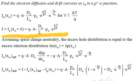
i don't get it why the whole current is like
that
can u explain in detail?
Homework Answers
Its because ,
At any point in the quasi neutral region, the total current is given by
I_total= I_n +I_p
where I_n is current due to elecron and I_p is due to holes.
Now each current component corresponding to holes or electrons is made up of drift and diffusion currents.
And since it is p+ n diode , the n type will be minority carrier in the p region where x_n=0 , so they are approximating total current at the edge to be that of only holes and current due to electrons is assumed to be zero.
Hence you are seeing that,.
Add Answer to:
i don't get it why the whole current is like that can u explain in detail? Find the electron diffusion and drift...
A3. (a) Draw a band diagram and a cross-sectional diagram of an abrupt p-n junction0Marks] with N...
 a3. (a) Draw a band diagram and a cross-sectional diagram of an abrupt p-n junction0Marks] with N>N at thermal equilibrium at 300K and label the following: () Diffusion currents, (i) Drift currents (ii) Fermi level, (iv) SCR, (v) QNR, (vi) Contact potential with polarity, (vi) Electric field distribution in the SCR, (vii) Electrostatic potential distribution in SCR, (ix) SCR charges, and (x) SCR penetration into the p-and n sides. (b) In a p'-n junction at 300K, the n side has...
i. l e blank(s). A gap suggest two-word in your answer Drift current in semiconductors is...
 i. l e blank(s). A gap suggest two-word in your answer Drift current in semiconductors is due to electric [20] tield. Carriers in the band are referred to as statistics is applied to electrons in The semiconductors. The position and principle states that we cannot simultaneously determine the of electrons. Vy is a . while w is a number and Current in the conduction is due to the flow of Extrinsic semiconductors are vii. viii. The wave function in Schrodinger's...
Taking pure silicon (Si) as an example, explain what is meant by the terms electron-hole generation...
 Taking pure silicon (Si) as an example, explain what is meant by the terms electron-hole generation and recombination, how they affect the electrical conductivity, and define what is meant by the "intrinsic carrier density", n. [5 marks] Q3. a) b) With the aid of both lattice and energy band diagrams, explain how n-type doping of Si is achieved and state two types of suitable dopant atoms. [7 marks] c) An n-type region on a Si wafer has a donor concentration...
Can I please get some help on this. Have to use excel answering these M Office...
 Can I please get some help on this. Have to use excel
answering these
M Office Update To keep up-to-date with security updates, and improvements, choose Check for Updates K9 Xf A. Formular Adid. Multiply. Divide; Cel Referencing Using Excel to Compute Multiple Product Break-Even Points Student Work Area Required:Provide input into cated in yellow in this template. Use the PROBLEM Die Candle Supplysis. The sales mi ( spermitage of dollar led the brink of its reprodact, and it wolfred...
Can I please get some help on this. Have to use excel
answering these
M Office Update To keep up-to-date with security updates, and improvements, choose Check for Updates K9 Xf A. Formular Adid. Multiply. Divide; Cel Referencing Using Excel to Compute Multiple Product Break-Even Points Student Work Area Required:Provide input into cated in yellow in this template. Use the PROBLEM Die Candle Supplysis. The sales mi ( spermitage of dollar led the brink of its reprodact, and it wolfred...
 a3. (a) Draw a band diagram and a cross-sectional diagram of an abrupt p-n junction0Marks] with N>N at thermal equilibrium at 300K and label the following: () Diffusion currents, (i) Drift currents (ii) Fermi level, (iv) SCR, (v) QNR, (vi) Contact potential with polarity, (vi) Electric field distribution in the SCR, (vii) Electrostatic potential distribution in SCR, (ix) SCR charges, and (x) SCR penetration into the p-and n sides. (b) In a p'-n junction at 300K, the n side has...
 i. l e blank(s). A gap suggest two-word in your answer Drift current in semiconductors is due to electric [20] tield. Carriers in the band are referred to as statistics is applied to electrons in The semiconductors. The position and principle states that we cannot simultaneously determine the of electrons. Vy is a . while w is a number and Current in the conduction is due to the flow of Extrinsic semiconductors are vii. viii. The wave function in Schrodinger's...
 Taking pure silicon (Si) as an example, explain what is meant by the terms electron-hole generation and recombination, how they affect the electrical conductivity, and define what is meant by the "intrinsic carrier density", n. [5 marks] Q3. a) b) With the aid of both lattice and energy band diagrams, explain how n-type doping of Si is achieved and state two types of suitable dopant atoms. [7 marks] c) An n-type region on a Si wafer has a donor concentration...
 Can I please get some help on this. Have to use excel
answering these
M Office Update To keep up-to-date with security updates, and improvements, choose Check for Updates K9 Xf A. Formular Adid. Multiply. Divide; Cel Referencing Using Excel to Compute Multiple Product Break-Even Points Student Work Area Required:Provide input into cated in yellow in this template. Use the PROBLEM Die Candle Supplysis. The sales mi ( spermitage of dollar led the brink of its reprodact, and it wolfred...
Can I please get some help on this. Have to use excel
answering these
M Office Update To keep up-to-date with security updates, and improvements, choose Check for Updates K9 Xf A. Formular Adid. Multiply. Divide; Cel Referencing Using Excel to Compute Multiple Product Break-Even Points Student Work Area Required:Provide input into cated in yellow in this template. Use the PROBLEM Die Candle Supplysis. The sales mi ( spermitage of dollar led the brink of its reprodact, and it wolfred...
Most questions answered within 3 hours.
-
An MNE is this kind of industry when competition in one country
is essentially independent of...
asked 13 minutes ago -
. For this set of questions, determine what
proportion of a normal distribution is located betweeneach...
asked 48 minutes ago -
A college student is employed as a door-to-door newspaper
salesman. Historical data suggests that the student...
asked 1 hour ago -
MATLAB HW 11 problem using Switch Case and Input commands
Write a script file that calculates...
asked 1 hour ago -
Considering gravitational time dilation, calculate the time that
passes in Earth’s surface while 1 hour passes...
asked 2 hours ago -
Minitab Problem: Take the Lake Hume June rainfall data and find
use the processes outlined in...
asked 2 hours ago -
X Company is trying to decide whether to continue using old
equipment to make Product A...
asked 3 hours ago -
IN PYTHON ONLY !! Program 2: Re-work
program #5 (WeeklyHours) from the previous assignment such that...
asked 3 hours ago -
The average length of time between arrivals at a turnpike
toll-booth is 26 seconds. What is...
asked 5 hours ago -
(a) A piston at 6.1 atm contains a gas that occupies a volume of
3.5 L....
asked 6 hours ago -
Please answer true or false. Words
cannot be changed or added in to make it true...
asked 6 hours ago -
An empty test tube weighs 15.923 grams. Then,
MgCl2•6H2O is added into the test tube. After...
asked 6 hours ago