
Q2)
Please show all working
Thank you :)
Homework Answers

Add Answer to:
Q2) Please show all working Thank you :) Question 2 (25 Marks) (a) (6 Marks) Bias...
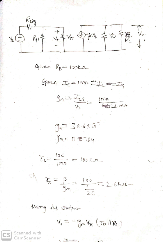
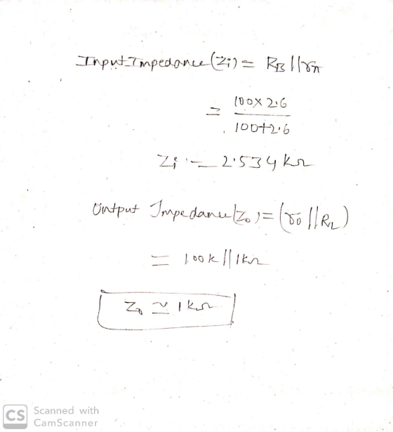
Consider the following coupled amplifier circuit using BJT with the following specifications: VBE 0.7V, VA 80V,...
 Consider the following coupled amplifier circuit using BJT with the following specifications: VBE 0.7V, VA 80V, fr 800MHz, c 0.8pF, Cci 0.01uF, Cc2-0.luF, CE-10uF, Submit the following: 1. Hand calculation for the mid-band gain AM [Vo Vsig], lower 3dB frequency fi and upper 2. Spice simulation of the circuit: Submit:l) SPICE input file, 2) Probe output file showing 3. Compare the hand calculated and simulated values described above in a table and last 3dB frequency fH, and gain-bandwidth product mid-band...
1-Clear handwriting 2-Correct answer 3-Organized 4-answer all the questions Please Problem 2 On the circuit on...
 1-Clear handwriting
2-Correct answer
3-Organized
4-answer all the questions
Please
Problem 2 On the circuit on Figure P2, transi stor Q1 has a threshold voltage of Vt = 2 V and a transconductance parameter of k = 100 mA/V2. Note that Vcc = -Vee = 4.5 V. Moreover, capacitors C1, C2, and C3 can be assumed to be very large VDD 4.5.0 R3 25kQ R1 300kn C2 Vout C1 Rsig Q1 1k0 R2 200kn Vsig (R4 2kQ C3 -4.5V VSS...
1-Clear handwriting
2-Correct answer
3-Organized
4-answer all the questions
Please
Problem 2 On the circuit on Figure P2, transi stor Q1 has a threshold voltage of Vt = 2 V and a transconductance parameter of k = 100 mA/V2. Note that Vcc = -Vee = 4.5 V. Moreover, capacitors C1, C2, and C3 can be assumed to be very large VDD 4.5.0 R3 25kQ R1 300kn C2 Vout C1 Rsig Q1 1k0 R2 200kn Vsig (R4 2kQ C3 -4.5V VSS...
EEET2255 Electtronics Page 6 of6 QUESTION 5 [25 marks Assume that the transistor in Figure 5...
 EEET2255 Electtronics Page 6 of6 QUESTION 5 [25 marks Assume that the transistor in Figure 5 is biasead with l 2.0mA and that its small-signal parameters are as follows: 150. C 6.0pF. C 15pF, Early voltage VA 150V 12 Figure 5 Determine the break (-3dB) frequencies that define the bandpass characteristic of this amplifier: 5.a at the low frequency and. 1.3KH2 [12 marks) at the high frequency end 5.b 3.4MHz (wo poles are close tagether, so need to combine as...
QUESTION 2 [Total 20 Marks] Figure 2.1 presents the BJT amplifier's DC biasing voltages (PSpice Biasing...
 QUESTION 2 [Total 20 Marks] Figure 2.1 presents the BJT amplifier's DC biasing voltages (PSpice Biasing Point simulation). In your evaluation assume that ANSWER: the output resistance of the BJT Q1 is infinite a)-29.4x10⁵ A/V Establish the slope of the DC load line Establish the slope of the AC load line Sketch the DC and AC load lines directly on the transistor's Ic vs Vc plot provided in Figure 2.2 a) b) c) [3 marks] 3 marks] b)-75.8x10⁻³ A/ [10...
please pick one of the multiple choice options above. show all work, thank you Question 9...
 please pick one of the multiple choice options above.
show all work, thank you
Question 9 CIRCUIT X/FIG.9 (5 Marks) Statement: Consider the RC-coupled amplifier circuit illustrated in Fig. 9 (CIRCUIT X). Sketching relevant output (Vc-Ic) characteristics that decide Q-point coordinates and DC load-line details (of the NPN-BJT/Si circuit of Fig. 9 of Circuit X) Further, establish an appropriate AC-load line and decide the maximum swing of the output voltage across Rload with respect to the Q-point. Assume the input...
please pick one of the multiple choice options above.
show all work, thank you
Question 9 CIRCUIT X/FIG.9 (5 Marks) Statement: Consider the RC-coupled amplifier circuit illustrated in Fig. 9 (CIRCUIT X). Sketching relevant output (Vc-Ic) characteristics that decide Q-point coordinates and DC load-line details (of the NPN-BJT/Si circuit of Fig. 9 of Circuit X) Further, establish an appropriate AC-load line and decide the maximum swing of the output voltage across Rload with respect to the Q-point. Assume the input...
ASAP! Please answer this question showing steps for thumb up! Question 1 (4 Marks) Q.A. 1...
 ASAP! Please answer this question showing steps for
thumb up!
Question 1 (4 Marks) Q.A. 1 -Statement: DC biasing of a CE amplifier circuit is as in Fig. Q.1. Assume the parameters, Vcc = 18 volt, RE = 500 ohm; B = 125; RL = 1000 ohm, Rc =1500 ohm and source resistance and Rs 1500 ohm. The amplifier is excited by a source, vs(t) = Vm * sin(2teft) with Vm = 25 mV peak and f = 1000 Hz;...
ASAP! Please answer this question showing steps for
thumb up!
Question 1 (4 Marks) Q.A. 1 -Statement: DC biasing of a CE amplifier circuit is as in Fig. Q.1. Assume the parameters, Vcc = 18 volt, RE = 500 ohm; B = 125; RL = 1000 ohm, Rc =1500 ohm and source resistance and Rs 1500 ohm. The amplifier is excited by a source, vs(t) = Vm * sin(2teft) with Vm = 25 mV peak and f = 1000 Hz;...
choose one of the multiple choice answers above. please show all work Question: 10 CIRCUIT Y...
 choose one of the multiple choice answers above.
please show all work
Question: 10 CIRCUIT Y FIG.10 (5 Marks) Statement: Consider the RC-coupled amplifier circuit illustrated in Fig. 10 (CIRCUIT Y). Sketching relevant output (Vc-Ic) characteristics, decide Q-point coordinates and DC load-line details (of the NPN-BJT/Si circuit of Fig. 10 of Circuit Y). Further, establish an appropriate AC-load line and decide the maximum swing of the output voltage across Rload with respect to the Q-point. Assume the input signal at...
choose one of the multiple choice answers above.
please show all work
Question: 10 CIRCUIT Y FIG.10 (5 Marks) Statement: Consider the RC-coupled amplifier circuit illustrated in Fig. 10 (CIRCUIT Y). Sketching relevant output (Vc-Ic) characteristics, decide Q-point coordinates and DC load-line details (of the NPN-BJT/Si circuit of Fig. 10 of Circuit Y). Further, establish an appropriate AC-load line and decide the maximum swing of the output voltage across Rload with respect to the Q-point. Assume the input signal at...
Electronics1. It's a multiple choices question. use the formula sheet if needed (the last picture). Question:...
 Electronics1. It's a multiple choices question. use the
formula sheet if needed (the last picture).
Question: 10 CIRCUIT Y/FIG.10 (5 Marks) Statement: Consider the RC-coupled amplifier circuit illustrated in Fig. 10 (CIRCUIT Y). Sketching relevant output (Vc-le) characteristics, decide Q-point coordinates and DC load-line details of the NPN-BJT/Si circuit of Fig.10 of Circuit Y). Further, establish an appropriate AC-load line and decide the maximum swing of the output voltage across Road with respect to the Q-point. Assume the input signal...
Electronics1. It's a multiple choices question. use the
formula sheet if needed (the last picture).
Question: 10 CIRCUIT Y/FIG.10 (5 Marks) Statement: Consider the RC-coupled amplifier circuit illustrated in Fig. 10 (CIRCUIT Y). Sketching relevant output (Vc-le) characteristics, decide Q-point coordinates and DC load-line details of the NPN-BJT/Si circuit of Fig.10 of Circuit Y). Further, establish an appropriate AC-load line and decide the maximum swing of the output voltage across Road with respect to the Q-point. Assume the input signal...
Problem 3: Design Problem On Figure P3a, you have a Common Source (CS) n-channel MOSFET amplifier....
 Problem 3: Design Problem On Figure P3a, you have a Common Source (CS) n-channel MOSFET amplifier. Notice the absence of a source resistor Rsig and load resistor R. If we know how the present amplifier (the one on Figure P3a) behaves without Rsig and RL, we can infer its behaviors if Rsig and R were to be added. design the amplifier circuit on Figure P3a, i.e., you have to find appropriate values for RGj You are to RG,, RD, and...
please choose one of the answer choices above. Must show all work, thank you Question 2...
 please choose one of the answer choices above.
Must show all work, thank you
Question 2 CIRCUIT A2 (2.5 Marks) + Ver Rc Ic с IR Fig. 2: CIRCUIT A.2 Statement: Sketching relevant output (Vc-Ic) characteristics decide on Q-point coordinates and DC load-line details: That is, determine DC operating conditions of the NPN-BJT/Si circuit of Fig.2 (denoting the type Circuit A2). Assume the following: Vcc= 24 volt; Rc = 5.0 k; RB = 1500 k and B = 125. Required...
please choose one of the answer choices above.
Must show all work, thank you
Question 2 CIRCUIT A2 (2.5 Marks) + Ver Rc Ic с IR Fig. 2: CIRCUIT A.2 Statement: Sketching relevant output (Vc-Ic) characteristics decide on Q-point coordinates and DC load-line details: That is, determine DC operating conditions of the NPN-BJT/Si circuit of Fig.2 (denoting the type Circuit A2). Assume the following: Vcc= 24 volt; Rc = 5.0 k; RB = 1500 k and B = 125. Required...
 Consider the following coupled amplifier circuit using BJT with the following specifications: VBE 0.7V, VA 80V, fr 800MHz, c 0.8pF, Cci 0.01uF, Cc2-0.luF, CE-10uF, Submit the following: 1. Hand calculation for the mid-band gain AM [Vo Vsig], lower 3dB frequency fi and upper 2. Spice simulation of the circuit: Submit:l) SPICE input file, 2) Probe output file showing 3. Compare the hand calculated and simulated values described above in a table and last 3dB frequency fH, and gain-bandwidth product mid-band...
 1-Clear handwriting
2-Correct answer
3-Organized
4-answer all the questions
Please
Problem 2 On the circuit on Figure P2, transi stor Q1 has a threshold voltage of Vt = 2 V and a transconductance parameter of k = 100 mA/V2. Note that Vcc = -Vee = 4.5 V. Moreover, capacitors C1, C2, and C3 can be assumed to be very large VDD 4.5.0 R3 25kQ R1 300kn C2 Vout C1 Rsig Q1 1k0 R2 200kn Vsig (R4 2kQ C3 -4.5V VSS...
1-Clear handwriting
2-Correct answer
3-Organized
4-answer all the questions
Please
Problem 2 On the circuit on Figure P2, transi stor Q1 has a threshold voltage of Vt = 2 V and a transconductance parameter of k = 100 mA/V2. Note that Vcc = -Vee = 4.5 V. Moreover, capacitors C1, C2, and C3 can be assumed to be very large VDD 4.5.0 R3 25kQ R1 300kn C2 Vout C1 Rsig Q1 1k0 R2 200kn Vsig (R4 2kQ C3 -4.5V VSS...
 EEET2255 Electtronics Page 6 of6 QUESTION 5 [25 marks Assume that the transistor in Figure 5 is biasead with l 2.0mA and that its small-signal parameters are as follows: 150. C 6.0pF. C 15pF, Early voltage VA 150V 12 Figure 5 Determine the break (-3dB) frequencies that define the bandpass characteristic of this amplifier: 5.a at the low frequency and. 1.3KH2 [12 marks) at the high frequency end 5.b 3.4MHz (wo poles are close tagether, so need to combine as...
 QUESTION 2 [Total 20 Marks] Figure 2.1 presents the BJT amplifier's DC biasing voltages (PSpice Biasing Point simulation). In your evaluation assume that ANSWER: the output resistance of the BJT Q1 is infinite a)-29.4x10⁵ A/V Establish the slope of the DC load line Establish the slope of the AC load line Sketch the DC and AC load lines directly on the transistor's Ic vs Vc plot provided in Figure 2.2 a) b) c) [3 marks] 3 marks] b)-75.8x10⁻³ A/ [10...
 please pick one of the multiple choice options above.
show all work, thank you
Question 9 CIRCUIT X/FIG.9 (5 Marks) Statement: Consider the RC-coupled amplifier circuit illustrated in Fig. 9 (CIRCUIT X). Sketching relevant output (Vc-Ic) characteristics that decide Q-point coordinates and DC load-line details (of the NPN-BJT/Si circuit of Fig. 9 of Circuit X) Further, establish an appropriate AC-load line and decide the maximum swing of the output voltage across Rload with respect to the Q-point. Assume the input...
please pick one of the multiple choice options above.
show all work, thank you
Question 9 CIRCUIT X/FIG.9 (5 Marks) Statement: Consider the RC-coupled amplifier circuit illustrated in Fig. 9 (CIRCUIT X). Sketching relevant output (Vc-Ic) characteristics that decide Q-point coordinates and DC load-line details (of the NPN-BJT/Si circuit of Fig. 9 of Circuit X) Further, establish an appropriate AC-load line and decide the maximum swing of the output voltage across Rload with respect to the Q-point. Assume the input...
 ASAP! Please answer this question showing steps for
thumb up!
Question 1 (4 Marks) Q.A. 1 -Statement: DC biasing of a CE amplifier circuit is as in Fig. Q.1. Assume the parameters, Vcc = 18 volt, RE = 500 ohm; B = 125; RL = 1000 ohm, Rc =1500 ohm and source resistance and Rs 1500 ohm. The amplifier is excited by a source, vs(t) = Vm * sin(2teft) with Vm = 25 mV peak and f = 1000 Hz;...
ASAP! Please answer this question showing steps for
thumb up!
Question 1 (4 Marks) Q.A. 1 -Statement: DC biasing of a CE amplifier circuit is as in Fig. Q.1. Assume the parameters, Vcc = 18 volt, RE = 500 ohm; B = 125; RL = 1000 ohm, Rc =1500 ohm and source resistance and Rs 1500 ohm. The amplifier is excited by a source, vs(t) = Vm * sin(2teft) with Vm = 25 mV peak and f = 1000 Hz;...
 choose one of the multiple choice answers above.
please show all work
Question: 10 CIRCUIT Y FIG.10 (5 Marks) Statement: Consider the RC-coupled amplifier circuit illustrated in Fig. 10 (CIRCUIT Y). Sketching relevant output (Vc-Ic) characteristics, decide Q-point coordinates and DC load-line details (of the NPN-BJT/Si circuit of Fig. 10 of Circuit Y). Further, establish an appropriate AC-load line and decide the maximum swing of the output voltage across Rload with respect to the Q-point. Assume the input signal at...
choose one of the multiple choice answers above.
please show all work
Question: 10 CIRCUIT Y FIG.10 (5 Marks) Statement: Consider the RC-coupled amplifier circuit illustrated in Fig. 10 (CIRCUIT Y). Sketching relevant output (Vc-Ic) characteristics, decide Q-point coordinates and DC load-line details (of the NPN-BJT/Si circuit of Fig. 10 of Circuit Y). Further, establish an appropriate AC-load line and decide the maximum swing of the output voltage across Rload with respect to the Q-point. Assume the input signal at...
 Electronics1. It's a multiple choices question. use the
formula sheet if needed (the last picture).
Question: 10 CIRCUIT Y/FIG.10 (5 Marks) Statement: Consider the RC-coupled amplifier circuit illustrated in Fig. 10 (CIRCUIT Y). Sketching relevant output (Vc-le) characteristics, decide Q-point coordinates and DC load-line details of the NPN-BJT/Si circuit of Fig.10 of Circuit Y). Further, establish an appropriate AC-load line and decide the maximum swing of the output voltage across Road with respect to the Q-point. Assume the input signal...
Electronics1. It's a multiple choices question. use the
formula sheet if needed (the last picture).
Question: 10 CIRCUIT Y/FIG.10 (5 Marks) Statement: Consider the RC-coupled amplifier circuit illustrated in Fig. 10 (CIRCUIT Y). Sketching relevant output (Vc-le) characteristics, decide Q-point coordinates and DC load-line details of the NPN-BJT/Si circuit of Fig.10 of Circuit Y). Further, establish an appropriate AC-load line and decide the maximum swing of the output voltage across Road with respect to the Q-point. Assume the input signal...
 Problem 3: Design Problem On Figure P3a, you have a Common Source (CS) n-channel MOSFET amplifier. Notice the absence of a source resistor Rsig and load resistor R. If we know how the present amplifier (the one on Figure P3a) behaves without Rsig and RL, we can infer its behaviors if Rsig and R were to be added. design the amplifier circuit on Figure P3a, i.e., you have to find appropriate values for RGj You are to RG,, RD, and...
 please choose one of the answer choices above.
Must show all work, thank you
Question 2 CIRCUIT A2 (2.5 Marks) + Ver Rc Ic с IR Fig. 2: CIRCUIT A.2 Statement: Sketching relevant output (Vc-Ic) characteristics decide on Q-point coordinates and DC load-line details: That is, determine DC operating conditions of the NPN-BJT/Si circuit of Fig.2 (denoting the type Circuit A2). Assume the following: Vcc= 24 volt; Rc = 5.0 k; RB = 1500 k and B = 125. Required...
please choose one of the answer choices above.
Must show all work, thank you
Question 2 CIRCUIT A2 (2.5 Marks) + Ver Rc Ic с IR Fig. 2: CIRCUIT A.2 Statement: Sketching relevant output (Vc-Ic) characteristics decide on Q-point coordinates and DC load-line details: That is, determine DC operating conditions of the NPN-BJT/Si circuit of Fig.2 (denoting the type Circuit A2). Assume the following: Vcc= 24 volt; Rc = 5.0 k; RB = 1500 k and B = 125. Required...
Most questions answered within 3 hours.
-
Please answer true or false. Words
cannot be changed or added in to make it true...
asked 54 minutes ago -
An empty test tube weighs 15.923 grams. Then,
MgCl2•6H2O is added into the test tube. After...
asked 56 minutes ago -
(a) A piston at 6.1 atm contains a gas that occupies a volume of
3.5 L....
asked 55 minutes ago -
Assume memory access is 10 units of time and disk access is
10000 units of time....
asked 1 hour ago -
1. Are all good samples random?
2. Magazines often report surveys giving statistics such as “63%...
asked 1 hour ago -
Under all the various types of market structures, firms
must eventually earn some economic profits for...
asked 1 hour ago -
Consider the following fitness regime for a single locus trait
with two co-dominant alleles: w11 =...
asked 1 hour ago -
A large cable company reports the following.
80% of its customers subscribe to its cable TV...
asked 1 hour ago -
Please answer the question in brief.
Discuss the role of ERP in organizations. Are ERP tools...
asked 1 hour ago -
Discuss the pros and cons of collaborative software such
as SameTime. Does it increase productivity? What...
asked 1 hour ago -
Buying your in-laws a gift because it’s expected is
due to the ____________ motive of gift-giving....
asked 1 hour ago -
Calculate the expected value, the variance, and the standard
deviation of the given random variable X....
asked 2 hours ago