

Homework Answers


Add Answer to:
show all the steps
(35p) 5. For this single transistor amplifier, the transistor parameters are VI...
For the amplifier configuration in Figure 4.1, the transistor parameters are; loss 10 mA, Vp 5...
 For the amplifier configuration in Figure 4.1, the transistor parameters are; loss 10 mA, Vp 5 V and 0.01 V. The circuit parameters are; VDo 12 V, Rs 1.2 kn, Ri-265 k, R2 165 k, and RL-0.5 k [Bagi tatarajah penguat dalam Rajah 4.1, parameter transistor adalah; Inss 10 m, V- sV dan à-0.01 Parameter litar adalah; V 12 V, Rs 1.2 k R 265 R-165 k, dan R-0.5 ko VDD Rin R Ro Cc Cc2 RL R2 Rs +...
Please Solve ALL parts. For the amplifier below, the MOSFET has the following parameters: VIV, k...
 Please Solve ALL parts.
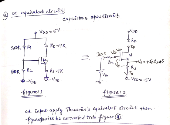
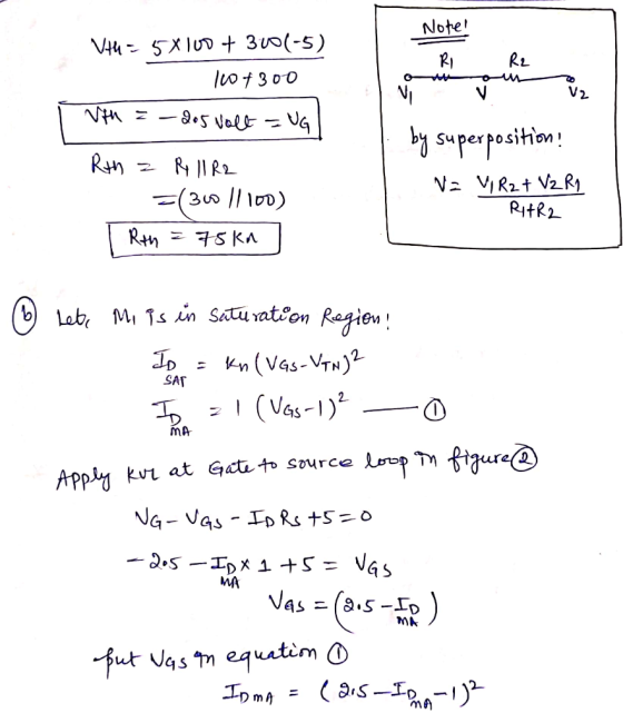
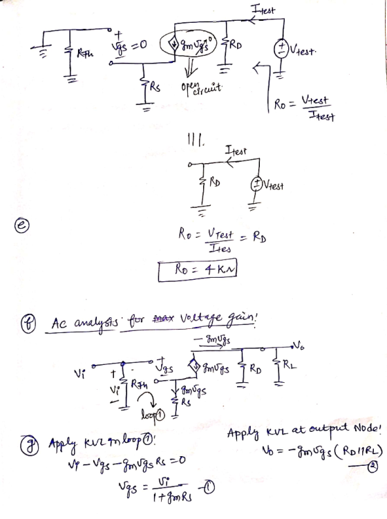
For the amplifier below, the MOSFET has the following parameters: VIV, k 1) Show (prove) that the transistor operates in the saturation mode 2) Determine the operating point by finding In and VDs 3) Assume infinite values for the coupling capacitors and draw a small signal model for this amplifier ) Find gm and ro 5) Find the voltage gain (vo/vi) Find Ri 7) Find the current gain (ioli) VDD +12V RD- 10k2 Vo Vi lmA...
Please Solve ALL parts.
For the amplifier below, the MOSFET has the following parameters: VIV, k 1) Show (prove) that the transistor operates in the saturation mode 2) Determine the operating point by finding In and VDs 3) Assume infinite values for the coupling capacitors and draw a small signal model for this amplifier ) Find gm and ro 5) Find the voltage gain (vo/vi) Find Ri 7) Find the current gain (ioli) VDD +12V RD- 10k2 Vo Vi lmA...
Small-Signal Mid- Band Voltage Gain (Range) Transistors Amplifier Confiaurations +2) to (+5 P-JFET Common Gate By referring to a specific transistor datasheet, design a single stage amplifier circuit...
 Small-Signal Mid- Band Voltage Gain (Range) Transistors Amplifier Confiaurations +2) to (+5 P-JFET Common Gate By referring to a specific transistor datasheet, design a single stage amplifier circuit with the following specifications. Include in your design, (i) the amplifier circuit, (ii) DC & AC equivalent circuits, (ii) DC & AC analysis and (iv) frequency response. State your assumptions, if any.
Small-Signal Mid- Band Voltage Gain (Range) Transistors Amplifier Confiaurations +2) to (+5 P-JFET Common Gate By referring to a specific...
Small-Signal Mid- Band Voltage Gain (Range) Transistors Amplifier Confiaurations +2) to (+5 P-JFET Common Gate By referring to a specific transistor datasheet, design a single stage amplifier circuit with the following specifications. Include in your design, (i) the amplifier circuit, (ii) DC & AC equivalent circuits, (ii) DC & AC analysis and (iv) frequency response. State your assumptions, if any.
Small-Signal Mid- Band Voltage Gain (Range) Transistors Amplifier Confiaurations +2) to (+5 P-JFET Common Gate By referring to a specific...
Laboratory 2: Transistor circuit characteristics A. Objectives: 1. To study the basic characteris...
 Laboratory 2: Transistor circuit characteristics A. Objectives: 1. To study the basic characteristics of a transistor circuit. 2. To study the bias circuit of a transistor circuit. B. Apparatus: 1. DC Power supply 2. Experimental boards and corresponding components 3. Electronic calculator (prepared by students) 4. Digital camera (prepared by students for photo taking of the experimental results) 5. Laptop computer with the software PicoScope 6 and Microsoft Word installed. 6. PicoScope PC Oscilloscope and its accessories. 7. Digital multi-meter....
Homework 4 Due: June 26, 2019, at 5 pm. Note: Show all steps required to get...
 Homework 4 Due: June 26, 2019, at 5 pm. Note: Show all steps required to get to your answers and make sure to box them. Writing down answers to questions asked without any explanation(s) will not do it. Clarity should be a priority Moreover, the assigned textbook for this class is Sedra and Smith, Microelectronic Circuits, Seventh Edition, Oxford University Press. Make sure you have the proper book Reminder: In class, we have expressed the overall voltage gain of a...
Homework 4 Due: June 26, 2019, at 5 pm. Note: Show all steps required to get...
 Homework 4 Due: June 26, 2019, at 5 pm. Note: Show all steps required to get to your answers and make sure to box them. Writing down answers to questions asked without any explanation(s) will not do it. Clarity should be a priority Moreover, the assigned textbook for this class is Sedra and Smith, Microelectronic Circuits, Seventh Edition, Oxford Univers ity Press. Make sure you have the proper book Reminder: In class, we have expressed the overall voltage gain of...
PLEASE SHOW ALL WORK AND TO FOLLOW DIRECTIONS. PLEASE USE PSPICE. STUDENT ID= 7220849 2. Using...
 PLEASE SHOW ALL WORK AND TO FOLLOW DIRECTIONS. PLEASE USE
PSPICE.
STUDENT ID= 7220849
2. Using a DC Sweep analysis to generate a table of values in the .OUT file: See Circuit 2 below: Let R1 through R6 equivalent to the digits 1 through 6 in your StudentID in k12 (use 10 k22 for a digit of 0). • For example, if your StudentID is 9870654 then R1 =9 kN, R2 =8 kN, R3 = 7kN, R4 = 10KN, R5...
PLEASE SHOW ALL WORK AND TO FOLLOW DIRECTIONS. PLEASE USE
PSPICE.
STUDENT ID= 7220849
2. Using a DC Sweep analysis to generate a table of values in the .OUT file: See Circuit 2 below: Let R1 through R6 equivalent to the digits 1 through 6 in your StudentID in k12 (use 10 k22 for a digit of 0). • For example, if your StudentID is 9870654 then R1 =9 kN, R2 =8 kN, R3 = 7kN, R4 = 10KN, R5...
 For the amplifier configuration in Figure 4.1, the transistor parameters are; loss 10 mA, Vp 5 V and 0.01 V. The circuit parameters are; VDo 12 V, Rs 1.2 kn, Ri-265 k, R2 165 k, and RL-0.5 k [Bagi tatarajah penguat dalam Rajah 4.1, parameter transistor adalah; Inss 10 m, V- sV dan à-0.01 Parameter litar adalah; V 12 V, Rs 1.2 k R 265 R-165 k, dan R-0.5 ko VDD Rin R Ro Cc Cc2 RL R2 Rs +...
 Please Solve ALL parts.
For the amplifier below, the MOSFET has the following parameters: VIV, k 1) Show (prove) that the transistor operates in the saturation mode 2) Determine the operating point by finding In and VDs 3) Assume infinite values for the coupling capacitors and draw a small signal model for this amplifier ) Find gm and ro 5) Find the voltage gain (vo/vi) Find Ri 7) Find the current gain (ioli) VDD +12V RD- 10k2 Vo Vi lmA...
Please Solve ALL parts.
For the amplifier below, the MOSFET has the following parameters: VIV, k 1) Show (prove) that the transistor operates in the saturation mode 2) Determine the operating point by finding In and VDs 3) Assume infinite values for the coupling capacitors and draw a small signal model for this amplifier ) Find gm and ro 5) Find the voltage gain (vo/vi) Find Ri 7) Find the current gain (ioli) VDD +12V RD- 10k2 Vo Vi lmA...
 Small-Signal Mid- Band Voltage Gain (Range) Transistors Amplifier Confiaurations +2) to (+5 P-JFET Common Gate By referring to a specific transistor datasheet, design a single stage amplifier circuit with the following specifications. Include in your design, (i) the amplifier circuit, (ii) DC & AC equivalent circuits, (ii) DC & AC analysis and (iv) frequency response. State your assumptions, if any.
Small-Signal Mid- Band Voltage Gain (Range) Transistors Amplifier Confiaurations +2) to (+5 P-JFET Common Gate By referring to a specific...
Small-Signal Mid- Band Voltage Gain (Range) Transistors Amplifier Confiaurations +2) to (+5 P-JFET Common Gate By referring to a specific transistor datasheet, design a single stage amplifier circuit with the following specifications. Include in your design, (i) the amplifier circuit, (ii) DC & AC equivalent circuits, (ii) DC & AC analysis and (iv) frequency response. State your assumptions, if any.
Small-Signal Mid- Band Voltage Gain (Range) Transistors Amplifier Confiaurations +2) to (+5 P-JFET Common Gate By referring to a specific...
 Laboratory 2: Transistor circuit characteristics A. Objectives: 1. To study the basic characteristics of a transistor circuit. 2. To study the bias circuit of a transistor circuit. B. Apparatus: 1. DC Power supply 2. Experimental boards and corresponding components 3. Electronic calculator (prepared by students) 4. Digital camera (prepared by students for photo taking of the experimental results) 5. Laptop computer with the software PicoScope 6 and Microsoft Word installed. 6. PicoScope PC Oscilloscope and its accessories. 7. Digital multi-meter....
 Homework 4 Due: June 26, 2019, at 5 pm. Note: Show all steps required to get to your answers and make sure to box them. Writing down answers to questions asked without any explanation(s) will not do it. Clarity should be a priority Moreover, the assigned textbook for this class is Sedra and Smith, Microelectronic Circuits, Seventh Edition, Oxford University Press. Make sure you have the proper book Reminder: In class, we have expressed the overall voltage gain of a...
 Homework 4 Due: June 26, 2019, at 5 pm. Note: Show all steps required to get to your answers and make sure to box them. Writing down answers to questions asked without any explanation(s) will not do it. Clarity should be a priority Moreover, the assigned textbook for this class is Sedra and Smith, Microelectronic Circuits, Seventh Edition, Oxford Univers ity Press. Make sure you have the proper book Reminder: In class, we have expressed the overall voltage gain of...
 PLEASE SHOW ALL WORK AND TO FOLLOW DIRECTIONS. PLEASE USE
PSPICE.
STUDENT ID= 7220849
2. Using a DC Sweep analysis to generate a table of values in the .OUT file: See Circuit 2 below: Let R1 through R6 equivalent to the digits 1 through 6 in your StudentID in k12 (use 10 k22 for a digit of 0). • For example, if your StudentID is 9870654 then R1 =9 kN, R2 =8 kN, R3 = 7kN, R4 = 10KN, R5...
PLEASE SHOW ALL WORK AND TO FOLLOW DIRECTIONS. PLEASE USE
PSPICE.
STUDENT ID= 7220849
2. Using a DC Sweep analysis to generate a table of values in the .OUT file: See Circuit 2 below: Let R1 through R6 equivalent to the digits 1 through 6 in your StudentID in k12 (use 10 k22 for a digit of 0). • For example, if your StudentID is 9870654 then R1 =9 kN, R2 =8 kN, R3 = 7kN, R4 = 10KN, R5...
Most questions answered within 3 hours.
-
This java code won't run and I can't figure out the problem with
it. Please help...
asked 32 minutes ago -
Trace the following recursive methods:
a) isPal with the string “abccda”
b) isAnBn with the string...
asked 1 hour ago -
1. Which of the following is false about photosynthesis?
A. ATP is the molecule used to...
asked 2 hours ago -
A simple random sample of size n=64 is obtained from a
population with a mean of...
asked 3 hours ago -
(2 dimensions, 1 object, 2 accelerations)
1) A projectile is thrown with a wind. The wind...
asked 4 hours ago -
Brian makes $34,100 per year. How much can Brian expect to
contribute to FICA taxes in...
asked 4 hours ago -
To buy a new house you must borrow $155,000. To do this you take
out a...
asked 5 hours ago -
Spacely Sprockets is evaluating the construction of a new plant
on land the company purchased for...
asked 6 hours ago -
1. Consider a linear regression model of y on K regressors and
an intercept.
(i) Describe...
asked 6 hours ago -
Enter a balanced equation for the reaction between hydrochloric
acid and sodium sulfite.
Express your answer...
asked 6 hours ago -
Give a regular expression describing the language
{x | x ∈ Σ* and x does not...
asked 6 hours ago -
Masses of 1.0 kg, 2.0 kg, and 3.0 kg are each separately subject
to a net...
asked 6 hours ago