
Homework Answers


 please give me likes
Thank you
Add Answer to:
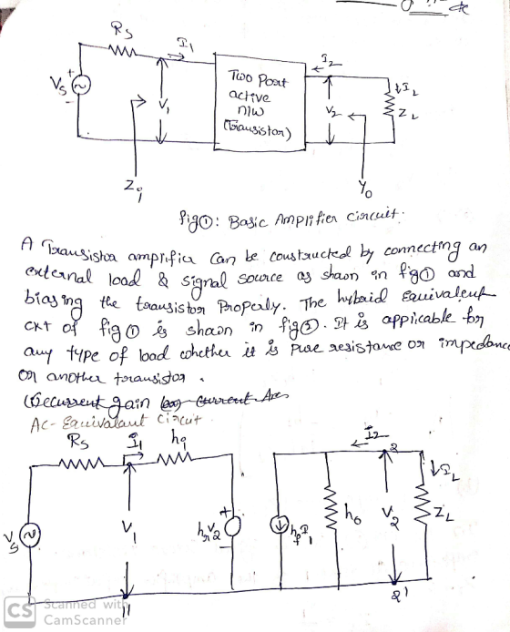
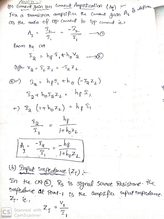
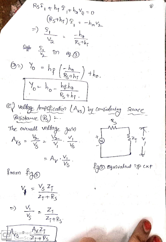
Small-Signal Mid- Band Voltage Gain (Range) Transistors Amplifier Confiaurations +2) to (+5 P-JFET Common Gate By referring to a specific transistor datasheet, design a single stage amplifier circuit...
3. Design a n-channel JFET C-S amplifier circuit for the following specifications Voltage Gain input resistance...
 3. Design a n-channel JFET C-S amplifier circuit for the following specifications Voltage Gain input resistance Ri-100kΩ Load resistanceR2k2 Given supply voltage VDD 20V Αν--10 Rss is fully bypassed The input source resistance Rs 02, Ipss-8mA and Vp4V Assume RD and R1 but must find R2 and RSS using the given specifications. Find the DC Operating Points values (VGs, ID and VDs) Draw the actual circuit and its ac equivalent circuit
3. Shown below is the small signal mid-band equivalent circuit of a MOSFET common gate amplifier....
 3. Shown below is the small signal mid-band equivalent circuit of a MOSFET common gate amplifier. Find the two-port z-parameters of this circuit in terms of the circuit components, ie. resistors and transconductance gm. m gs gs
IX With reference to the transistor amplifier shown in Figure QB4 below d For the bipolar transistor circuit of Figure QB4 the following DC bias conditions were measured: VB made. 1.6 V and VBE =0.6...
 IX With reference to the transistor amplifier shown in Figure QB4 below d For the bipolar transistor circuit of Figure QB4 the following DC bias conditions were measured: VB made. 1.6 V and VBE =0.6 V. Detemine the value for RA, stating any assumptions e) Using these same conditions, calculate the current in Re and deduce the current in Rc, stating any assumptions made. Hence find the voltage across Rc and explain whether this voltage is suitable for this amplifier...
Laboratory 2: Transistor circuit characteristics A. Objectives: 1. To study the basic characteris...
 Laboratory 2: Transistor circuit characteristics A. Objectives: 1. To study the basic characteristics of a transistor circuit. 2. To study the bias circuit of a transistor circuit. B. Apparatus: 1. DC Power supply 2. Experimental boards and corresponding components 3. Electronic calculator (prepared by students) 4. Digital camera (prepared by students for photo taking of the experimental results) 5. Laptop computer with the software PicoScope 6 and Microsoft Word installed. 6. PicoScope PC Oscilloscope and its accessories. 7. Digital multi-meter....
Design the CS amplifier in Fig. L7.17(a) to achieve a small-signal gain of at least 4,--5 V/V. Us...
 Design the CS amplifier in Fig. L7.17(a) to achieve a small-signal gain of at least 4,--5 V/V. Use supplies of V+--K = 15 V, Rsig-50 Ω, RL-10 kQ, and R1R2 = 10 kQ, and design the circuit to have ID-1 mA and a DC voltage at the gate Vo = 0 V. Use Cc,-CC2-CS-47 μF. What is the expected DC voltage at the source of the NMOS? C1 sig V. Rs sig
Design the CS amplifier in Fig. L7.17(a) to...
Design the CS amplifier in Fig. L7.17(a) to achieve a small-signal gain of at least 4,--5 V/V. Use supplies of V+--K = 15 V, Rsig-50 Ω, RL-10 kQ, and R1R2 = 10 kQ, and design the circuit to have ID-1 mA and a DC voltage at the gate Vo = 0 V. Use Cc,-CC2-CS-47 μF. What is the expected DC voltage at the source of the NMOS? C1 sig V. Rs sig
Design the CS amplifier in Fig. L7.17(a) to...
Problem 2 Consider the feedback amplifier circuit on Figure P2. The DC current gain of transistor Q3 is -100 1. What type of feedback (or what feedback topology) do we have on the circuit in Figure P...
 Problem 2 Consider the feedback amplifier circuit on Figure P2. The DC current gain of transistor Q3 is -100 1. What type of feedback (or what feedback topology) do we have on the circuit in Figure P2? 2. Draw the A-circuit. Express and compute the open-loop voltage gain A at mid-band frequency 3, Draw the γ-circuit. Express and compute the feedback factor γ 4. Express and compute the overall gain of the feedback amplifier Ap Express and compute the input...
(a) The figure below shows the small-signal equivalent circuit of a voltage amplifier. The open-circuit output...
 (a) The figure below shows the small-signal equivalent circuit of a voltage amplifier. The open-circuit output of the supply v10 V (i) Determine the resistances if the regulation should be less than 5 % when 1 W is being delivered to a resistive load connected across vo in the mid frequency range. If the low frequency 3dB point is at 1 kHz and the high frequency 3 dB point is 100 kHz what are the capacitance values. Assume the circuit...
Design a common-source MOSFET amplifier such that RG is a multiple of D = o.st mot...
 Design a common-source MOSFET amplifier such that RG is a multiple of D = o.st mot (Avol 15.02 VN RL = 17kr • Choose a sinusoidal signal voltage, Vsig, with Rsig = 400 kN to use as the input in this problem. Use 2 kHz as the frequency of your sinusoidal. This is a design problem so vsig will not be unique. Use V+ = 0.8 V, k = 5 mA/V2, and VA = 80 V for your MOSFET. Assume...
shows two versions of a common-emitter amplifier and (i Fig. 1 (a) Find the expression for the small-signal voltage gai...
 shows two versions of a common-emitter amplifier and (i Fig. 1 (a) Find the expression for the small-signal voltage gain of Fig. 1(i) in terms of relevant small- signal parameters. (b) Over what frequency range will the gain of the Fig. 1(i) circuit be the same as that of the Fig. 1(i) circuit? (c) Which of the two circuits will show less variation in its de biasing in the presence of processing or temperature variations? Justify your answer. (d) Explain,...
You are required to design a 2-stage voltage amplifier (find values for RE, RC1, RC2) to meet the following criteria: an...
 You are required to design a 2-stage voltage amplifier (find
values for RE, RC1, RC2) to meet the following criteria: an input
resistance of 400 kΩ and an overall voltage gain equal to or
greater than 250, with a resistor output load, RL. Use a
common-emitter with emitter degradation (RE) stage for the input,
followed by a commonemitter amplifier with bias current equal to
0.5 mA. (VCC = 20 V, βo = 200 and the DC levels of the first...
You are required to design a 2-stage voltage amplifier (find
values for RE, RC1, RC2) to meet the following criteria: an input
resistance of 400 kΩ and an overall voltage gain equal to or
greater than 250, with a resistor output load, RL. Use a
common-emitter with emitter degradation (RE) stage for the input,
followed by a commonemitter amplifier with bias current equal to
0.5 mA. (VCC = 20 V, βo = 200 and the DC levels of the first...
 3. Design a n-channel JFET C-S amplifier circuit for the following specifications Voltage Gain input resistance Ri-100kΩ Load resistanceR2k2 Given supply voltage VDD 20V Αν--10 Rss is fully bypassed The input source resistance Rs 02, Ipss-8mA and Vp4V Assume RD and R1 but must find R2 and RSS using the given specifications. Find the DC Operating Points values (VGs, ID and VDs) Draw the actual circuit and its ac equivalent circuit
 3. Shown below is the small signal mid-band equivalent circuit of a MOSFET common gate amplifier. Find the two-port z-parameters of this circuit in terms of the circuit components, ie. resistors and transconductance gm. m gs gs
 IX With reference to the transistor amplifier shown in Figure QB4 below d For the bipolar transistor circuit of Figure QB4 the following DC bias conditions were measured: VB made. 1.6 V and VBE =0.6 V. Detemine the value for RA, stating any assumptions e) Using these same conditions, calculate the current in Re and deduce the current in Rc, stating any assumptions made. Hence find the voltage across Rc and explain whether this voltage is suitable for this amplifier...
 Laboratory 2: Transistor circuit characteristics A. Objectives: 1. To study the basic characteristics of a transistor circuit. 2. To study the bias circuit of a transistor circuit. B. Apparatus: 1. DC Power supply 2. Experimental boards and corresponding components 3. Electronic calculator (prepared by students) 4. Digital camera (prepared by students for photo taking of the experimental results) 5. Laptop computer with the software PicoScope 6 and Microsoft Word installed. 6. PicoScope PC Oscilloscope and its accessories. 7. Digital multi-meter....
 Design the CS amplifier in Fig. L7.17(a) to achieve a small-signal gain of at least 4,--5 V/V. Use supplies of V+--K = 15 V, Rsig-50 Ω, RL-10 kQ, and R1R2 = 10 kQ, and design the circuit to have ID-1 mA and a DC voltage at the gate Vo = 0 V. Use Cc,-CC2-CS-47 μF. What is the expected DC voltage at the source of the NMOS? C1 sig V. Rs sig
Design the CS amplifier in Fig. L7.17(a) to...
Design the CS amplifier in Fig. L7.17(a) to achieve a small-signal gain of at least 4,--5 V/V. Use supplies of V+--K = 15 V, Rsig-50 Ω, RL-10 kQ, and R1R2 = 10 kQ, and design the circuit to have ID-1 mA and a DC voltage at the gate Vo = 0 V. Use Cc,-CC2-CS-47 μF. What is the expected DC voltage at the source of the NMOS? C1 sig V. Rs sig
Design the CS amplifier in Fig. L7.17(a) to...
 Problem 2 Consider the feedback amplifier circuit on Figure P2. The DC current gain of transistor Q3 is -100 1. What type of feedback (or what feedback topology) do we have on the circuit in Figure P2? 2. Draw the A-circuit. Express and compute the open-loop voltage gain A at mid-band frequency 3, Draw the γ-circuit. Express and compute the feedback factor γ 4. Express and compute the overall gain of the feedback amplifier Ap Express and compute the input...
 (a) The figure below shows the small-signal equivalent circuit of a voltage amplifier. The open-circuit output of the supply v10 V (i) Determine the resistances if the regulation should be less than 5 % when 1 W is being delivered to a resistive load connected across vo in the mid frequency range. If the low frequency 3dB point is at 1 kHz and the high frequency 3 dB point is 100 kHz what are the capacitance values. Assume the circuit...
 Design a common-source MOSFET amplifier such that RG is a multiple of D = o.st mot (Avol 15.02 VN RL = 17kr • Choose a sinusoidal signal voltage, Vsig, with Rsig = 400 kN to use as the input in this problem. Use 2 kHz as the frequency of your sinusoidal. This is a design problem so vsig will not be unique. Use V+ = 0.8 V, k = 5 mA/V2, and VA = 80 V for your MOSFET. Assume...
 shows two versions of a common-emitter amplifier and (i Fig. 1 (a) Find the expression for the small-signal voltage gain of Fig. 1(i) in terms of relevant small- signal parameters. (b) Over what frequency range will the gain of the Fig. 1(i) circuit be the same as that of the Fig. 1(i) circuit? (c) Which of the two circuits will show less variation in its de biasing in the presence of processing or temperature variations? Justify your answer. (d) Explain,...
 You are required to design a 2-stage voltage amplifier (find
values for RE, RC1, RC2) to meet the following criteria: an input
resistance of 400 kΩ and an overall voltage gain equal to or
greater than 250, with a resistor output load, RL. Use a
common-emitter with emitter degradation (RE) stage for the input,
followed by a commonemitter amplifier with bias current equal to
0.5 mA. (VCC = 20 V, βo = 200 and the DC levels of the first...
You are required to design a 2-stage voltage amplifier (find
values for RE, RC1, RC2) to meet the following criteria: an input
resistance of 400 kΩ and an overall voltage gain equal to or
greater than 250, with a resistor output load, RL. Use a
common-emitter with emitter degradation (RE) stage for the input,
followed by a commonemitter amplifier with bias current equal to
0.5 mA. (VCC = 20 V, βo = 200 and the DC levels of the first...
Most questions answered within 3 hours.
-
The USPS sells money orders identified by an 11 –digit number
x1, x2, …, x11. The...
asked 19 seconds from now -
Provide an example of equilibrium in relation to
Newton’s First and Second Laws. Explain your answer....
asked 38 seconds ago -
You are __________ to commit a Type I error using the 0.05 level
of significance than...
asked 19 minutes ago -
1. the following results are obtained:
200
kiwi
575 wild-type
What can we conclude about the...
asked 23 minutes ago -
Explain how you might use E. coli bacteria to produce human
growth hormone using the following:...
asked 24 minutes ago -
WHAT IS THE EFFEKT OF ADD K2CO3 TO ( METHANOL OG WATER)?
asked 38 minutes ago -
Calculate the cell potential, the equilibrium constant, and the
free-energy change for: Ca(s)+Mn2+(aq)(1M)⇌Ca2+(aq)(1M)+Mn(s) given
the following...
asked 36 minutes ago -
Determine the pH at the equivalence (stoichiometric) point in
the titration of 48 mL of 0.28...
asked 36 minutes ago -
11. In CPM/PERT, an activity that is on the critical path
A. has equal values for...
asked 43 minutes ago -
Using C++ :
A Pascals triangle row is constructed by looking at the previous
row and...
asked 1 hour ago -
With what speed will the fastest photoelectrons be emitted from
a surface whose threshold wavelength is...
asked 59 minutes ago -
The following slope distances and differences in elevations
between the tape ends were recorded for a...
asked 1 hour ago