
C1 sig V. Rs sig
Homework Answers
Summary - it is basic problem so I have shown step by step
solution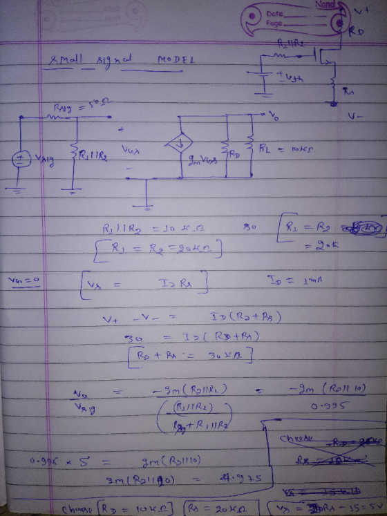
Add Answer to:
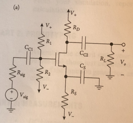
Design the CS amplifier in Fig. L7.17(a) to achieve a small-signal gain of at least 4,--5 V/V. Us...
Design a common-source MOSFET amplifier such that - Rg is a multiple of 10 - Id...
Design a common-source MOSFET amplifier such that - Rg is a multiple of 10 - Id = 0.52 mA - the amplifier input resistance is in the range of mega ohms - | Avo | = 16.7 V/V - RL = 20k - Vsig has a 2kHz frequency - Rsig = 400k, and is the input and the MOSFET has: Vt = 0.8V k = 5 mA/V^2 VA = 80 V Assume capacitors are shorted in the signal circuit and...
6.108 (d) Section 6.5: Discrete-Circuit Amplifiers 6.107 Calculate overall voltage gain G, of a 3 mA/V, ro= = 1...
 6.108 (d)
Section 6.5: Discrete-Circuit Amplifiers 6.107 Calculate overall voltage gain G, of a 3 mA/V, ro= = 10 MS2. The amplifier is the common-source amplifier for which g 100 k2, RD 10 k2, and RG fed from a signal source with a Thevenin resistance of l M2, and the amplifier output is coupled of 20 k2 to a load resistance SIM 6.108 The NMOS transistor in the CS amplifier shown in Fig. P6.108 has V, = 0.7 V and...
6.108 (d)
Section 6.5: Discrete-Circuit Amplifiers 6.107 Calculate overall voltage gain G, of a 3 mA/V, ro= = 10 MS2. The amplifier is the common-source amplifier for which g 100 k2, RD 10 k2, and RG fed from a signal source with a Thevenin resistance of l M2, and the amplifier output is coupled of 20 k2 to a load resistance SIM 6.108 The NMOS transistor in the CS amplifier shown in Fig. P6.108 has V, = 0.7 V and...
3) CS amplifier shown below is biased by a constant-current source I. Let Rsig 0.5 M, RG -2 MQ, gm -3mA/V, Rp -20 k2, and RL 10 k2. Find the midband voltage gain and the lower 3-dB frequency with...
 3) CS amplifier shown below is biased by a constant-current source I. Let Rsig 0.5 M, RG -2 MQ, gm -3mA/V, Rp -20 k2, and RL 10 k2. Find the midband voltage gain and the lower 3-dB frequency with Cc 6.3 nF, Cc2-0.53 uF and Cs-6 uF. Rp C2 C F
3) CS amplifier shown below is biased by a constant-current source I. Let Rsig 0.5 M, RG -2 MQ, gm -3mA/V, Rp -20 k2, and RL 10 k2. Find...
3) CS amplifier shown below is biased by a constant-current source I. Let Rsig 0.5 M, RG -2 MQ, gm -3mA/V, Rp -20 k2, and RL 10 k2. Find the midband voltage gain and the lower 3-dB frequency with Cc 6.3 nF, Cc2-0.53 uF and Cs-6 uF. Rp C2 C F
3) CS amplifier shown below is biased by a constant-current source I. Let Rsig 0.5 M, RG -2 MQ, gm -3mA/V, Rp -20 k2, and RL 10 k2. Find...
Design a common-source MOSFET amplifier such that RG is a multiple of D = o.st mot...
 Design a common-source MOSFET amplifier such that RG is a multiple of D = o.st mot (Avol 15.02 VN RL = 17kr • Choose a sinusoidal signal voltage, Vsig, with Rsig = 400 kN to use as the input in this problem. Use 2 kHz as the frequency of your sinusoidal. This is a design problem so vsig will not be unique. Use V+ = 0.8 V, k = 5 mA/V2, and VA = 80 V for your MOSFET. Assume...
Q1. For the cascade amplifier circuit shown in Fig (1): a) What are the functions of the capacitors C, C2 and C3? And w...
 Q1. For the cascade amplifier circuit shown in Fig (1): a) What are the functions of the capacitors C, C2 and C3? And what are the functions of the capacitors Cs and CE? b) What are the functions of the resistors RD and Rc? c) Draw the DC biasing circuits for each stage. d) Find loa, VGsa, VDs and gm for the JFET stage (you may use either mathematical or graphical methods) e) Calculate l, Ic, le and Ve for...
Problem 1 -Integrated Common Source Amplifier: For the circuit in Fig.1, draw the small signal equivalent...
 Problem 1 -Integrated Common Source Amplifier: For the circuit in Fig.1, draw the small signal equivalent circuit and find the following small signal values: gm1 go1 go2 Vout/Vin Rout You can assume that the overdrive voltage for all transistors is 0.2V and A for the NMOS and PMOS are 0.1V1 and 0.05V1 respectively. The drain source current of the transistors M1 and M2 is 20HA. All gate lengths of homework 3.) 0.5um. (The DC analysis for this circuit was done...
please I need details l and....Debate Club | Offic A) Theoretical Design Design a common emitter BJT amplifier with the following requirements: -Rin-10 K2, and Ro-45 ㏀ (Neglect the Early voltage...
 please I need details
l and....Debate Club | Offic A) Theoretical Design Design a common emitter BJT amplifier with the following requirements: -Rin-10 K2, and Ro-45 ㏀ (Neglect the Early voltage Effect) Vo/Vsig- Gv-40 VIV or 32 dB " VCC-9 V V, IC-1mA, VCE-3.25V and β-100 RL-40 kQ, Rsige I ka, R 1-3R2, and C1-C2-1 μF Voc RC C2 R1 Rsig C1 RL R2 RE B) Verify your design using Orcad Capture Pspice by doing 1) AC sweep (frequency response):...
please I need details
l and....Debate Club | Offic A) Theoretical Design Design a common emitter BJT amplifier with the following requirements: -Rin-10 K2, and Ro-45 ㏀ (Neglect the Early voltage Effect) Vo/Vsig- Gv-40 VIV or 32 dB " VCC-9 V V, IC-1mA, VCE-3.25V and β-100 RL-40 kQ, Rsige I ka, R 1-3R2, and C1-C2-1 μF Voc RC C2 R1 Rsig C1 RL R2 RE B) Verify your design using Orcad Capture Pspice by doing 1) AC sweep (frequency response):...
Exercise 7.37: Design the bias circuit for the CS amplifier. Assume the MOSFET is specified to...
 Exercise 7.37: Design the bias circuit for the CS amplifier. Assume the MOSFET is specified to have Vt 1 V, kn = 4mA/V2 and V4 = 100 V. Neglecting the Early effect, design for ID-0.5mA, VS= 3.5 V, VD6 V and VDD 15 V. Specify the values of RD and Rs If a current of 2 μΑ is used in the voltage divider, specify the values of RG1 and RG2. Give the values of the MOSFET parameters gm and ro...
Small-Signal Mid- Band Voltage Gain (Range) Transistors Amplifier Confiaurations +2) to (+5 P-JFET Common Gate By referring to a specific transistor datasheet, design a single stage amplifier circuit...
 Small-Signal Mid- Band Voltage Gain (Range) Transistors Amplifier Confiaurations +2) to (+5 P-JFET Common Gate By referring to a specific transistor datasheet, design a single stage amplifier circuit with the following specifications. Include in your design, (i) the amplifier circuit, (ii) DC & AC equivalent circuits, (ii) DC & AC analysis and (iv) frequency response. State your assumptions, if any.
Small-Signal Mid- Band Voltage Gain (Range) Transistors Amplifier Confiaurations +2) to (+5 P-JFET Common Gate By referring to a specific...
Small-Signal Mid- Band Voltage Gain (Range) Transistors Amplifier Confiaurations +2) to (+5 P-JFET Common Gate By referring to a specific transistor datasheet, design a single stage amplifier circuit with the following specifications. Include in your design, (i) the amplifier circuit, (ii) DC & AC equivalent circuits, (ii) DC & AC analysis and (iv) frequency response. State your assumptions, if any.
Small-Signal Mid- Band Voltage Gain (Range) Transistors Amplifier Confiaurations +2) to (+5 P-JFET Common Gate By referring to a specific...
D **7.124 The MOSFET in the amplifier circuit of Fig. P7.124 has V, 0.6 V and...
 D **7.124 The MOSFET in the amplifier circuit of Fig. P7.124 has V, 0.6 V and 5 mA/V'. We shall assume that Vis sufficiently large so that we can ignore the Early effect. The input signal v has a zero average. (a) It is required to bias the transistor to operate at an overdrive voltage 0.2 V. What must the dc voltage at the drain be? Calculate the dc drain current Ip. What value must Rp have? (b) Calculate the...
 6.108 (d)
Section 6.5: Discrete-Circuit Amplifiers 6.107 Calculate overall voltage gain G, of a 3 mA/V, ro= = 10 MS2. The amplifier is the common-source amplifier for which g 100 k2, RD 10 k2, and RG fed from a signal source with a Thevenin resistance of l M2, and the amplifier output is coupled of 20 k2 to a load resistance SIM 6.108 The NMOS transistor in the CS amplifier shown in Fig. P6.108 has V, = 0.7 V and...
6.108 (d)
Section 6.5: Discrete-Circuit Amplifiers 6.107 Calculate overall voltage gain G, of a 3 mA/V, ro= = 10 MS2. The amplifier is the common-source amplifier for which g 100 k2, RD 10 k2, and RG fed from a signal source with a Thevenin resistance of l M2, and the amplifier output is coupled of 20 k2 to a load resistance SIM 6.108 The NMOS transistor in the CS amplifier shown in Fig. P6.108 has V, = 0.7 V and...
 3) CS amplifier shown below is biased by a constant-current source I. Let Rsig 0.5 M, RG -2 MQ, gm -3mA/V, Rp -20 k2, and RL 10 k2. Find the midband voltage gain and the lower 3-dB frequency with Cc 6.3 nF, Cc2-0.53 uF and Cs-6 uF. Rp C2 C F
3) CS amplifier shown below is biased by a constant-current source I. Let Rsig 0.5 M, RG -2 MQ, gm -3mA/V, Rp -20 k2, and RL 10 k2. Find...
3) CS amplifier shown below is biased by a constant-current source I. Let Rsig 0.5 M, RG -2 MQ, gm -3mA/V, Rp -20 k2, and RL 10 k2. Find the midband voltage gain and the lower 3-dB frequency with Cc 6.3 nF, Cc2-0.53 uF and Cs-6 uF. Rp C2 C F
3) CS amplifier shown below is biased by a constant-current source I. Let Rsig 0.5 M, RG -2 MQ, gm -3mA/V, Rp -20 k2, and RL 10 k2. Find...
 Design a common-source MOSFET amplifier such that RG is a multiple of D = o.st mot (Avol 15.02 VN RL = 17kr • Choose a sinusoidal signal voltage, Vsig, with Rsig = 400 kN to use as the input in this problem. Use 2 kHz as the frequency of your sinusoidal. This is a design problem so vsig will not be unique. Use V+ = 0.8 V, k = 5 mA/V2, and VA = 80 V for your MOSFET. Assume...
 Q1. For the cascade amplifier circuit shown in Fig (1): a) What are the functions of the capacitors C, C2 and C3? And what are the functions of the capacitors Cs and CE? b) What are the functions of the resistors RD and Rc? c) Draw the DC biasing circuits for each stage. d) Find loa, VGsa, VDs and gm for the JFET stage (you may use either mathematical or graphical methods) e) Calculate l, Ic, le and Ve for...
 Problem 1 -Integrated Common Source Amplifier: For the circuit in Fig.1, draw the small signal equivalent circuit and find the following small signal values: gm1 go1 go2 Vout/Vin Rout You can assume that the overdrive voltage for all transistors is 0.2V and A for the NMOS and PMOS are 0.1V1 and 0.05V1 respectively. The drain source current of the transistors M1 and M2 is 20HA. All gate lengths of homework 3.) 0.5um. (The DC analysis for this circuit was done...
 please I need details
l and....Debate Club | Offic A) Theoretical Design Design a common emitter BJT amplifier with the following requirements: -Rin-10 K2, and Ro-45 ㏀ (Neglect the Early voltage Effect) Vo/Vsig- Gv-40 VIV or 32 dB " VCC-9 V V, IC-1mA, VCE-3.25V and β-100 RL-40 kQ, Rsige I ka, R 1-3R2, and C1-C2-1 μF Voc RC C2 R1 Rsig C1 RL R2 RE B) Verify your design using Orcad Capture Pspice by doing 1) AC sweep (frequency response):...
please I need details
l and....Debate Club | Offic A) Theoretical Design Design a common emitter BJT amplifier with the following requirements: -Rin-10 K2, and Ro-45 ㏀ (Neglect the Early voltage Effect) Vo/Vsig- Gv-40 VIV or 32 dB " VCC-9 V V, IC-1mA, VCE-3.25V and β-100 RL-40 kQ, Rsige I ka, R 1-3R2, and C1-C2-1 μF Voc RC C2 R1 Rsig C1 RL R2 RE B) Verify your design using Orcad Capture Pspice by doing 1) AC sweep (frequency response):...
 Exercise 7.37: Design the bias circuit for the CS amplifier. Assume the MOSFET is specified to have Vt 1 V, kn = 4mA/V2 and V4 = 100 V. Neglecting the Early effect, design for ID-0.5mA, VS= 3.5 V, VD6 V and VDD 15 V. Specify the values of RD and Rs If a current of 2 μΑ is used in the voltage divider, specify the values of RG1 and RG2. Give the values of the MOSFET parameters gm and ro...
 Small-Signal Mid- Band Voltage Gain (Range) Transistors Amplifier Confiaurations +2) to (+5 P-JFET Common Gate By referring to a specific transistor datasheet, design a single stage amplifier circuit with the following specifications. Include in your design, (i) the amplifier circuit, (ii) DC & AC equivalent circuits, (ii) DC & AC analysis and (iv) frequency response. State your assumptions, if any.
Small-Signal Mid- Band Voltage Gain (Range) Transistors Amplifier Confiaurations +2) to (+5 P-JFET Common Gate By referring to a specific...
Small-Signal Mid- Band Voltage Gain (Range) Transistors Amplifier Confiaurations +2) to (+5 P-JFET Common Gate By referring to a specific transistor datasheet, design a single stage amplifier circuit with the following specifications. Include in your design, (i) the amplifier circuit, (ii) DC & AC equivalent circuits, (ii) DC & AC analysis and (iv) frequency response. State your assumptions, if any.
Small-Signal Mid- Band Voltage Gain (Range) Transistors Amplifier Confiaurations +2) to (+5 P-JFET Common Gate By referring to a specific...
 D **7.124 The MOSFET in the amplifier circuit of Fig. P7.124 has V, 0.6 V and 5 mA/V'. We shall assume that Vis sufficiently large so that we can ignore the Early effect. The input signal v has a zero average. (a) It is required to bias the transistor to operate at an overdrive voltage 0.2 V. What must the dc voltage at the drain be? Calculate the dc drain current Ip. What value must Rp have? (b) Calculate the...
Most questions answered within 3 hours.
-
You have a 825.3 mL sample of 2.754 M HA (Ka =
4.49⋅10−4). Calculate the pH...
asked 14 minutes ago -
The blues made its way into many kinds of music. Eric Clapton,
The Beatles, and Elvis...
asked 2 hours ago -
8. A wave in a string has a wave function given by: y (x, t) =...
asked 1 hour ago -
If you’re standing at the bottom of a hill and asked to evaluate
it while being...
asked 3 hours ago -
1. Which region has taken the lead in the world of
e-waste handling?
a) European Union...
asked 3 hours ago -
A 8.15- g bullet from a 9-mm pistol has a velocity of 366.0 m/s.
It strikes...
asked 4 hours ago -
The outstanding bonds of Alpha Extracts have a yield to maturity
of 7.4 percent and a...
asked 4 hours ago -
The Problem: The Case of the Harmonizing Vacations
Your CEO is exploring partnering with a European...
asked 5 hours ago -
A chemical equation is balanced by adding coefficients in front
of some formulas so that the...
asked 5 hours ago -
From the literature (reference your sources): What are the
lattice parameters of calcite and aragonite? Why...
asked 6 hours ago -
Your system is rejecting the question am asking which is
preceded by a case study. It...
asked 6 hours ago -
3. On January 2, 2000, Larry creates a trust with himself as
trustee. Larry as trustee...
asked 6 hours ago