

(a) Construct and label the large-signal equivalent circuit (Bina dan labelkan litar setara isyarat-besar (2 Marks/ Markah) (b) By performing large-signal analysis, derive and determine the values of Dengan melakukan analisis isyarat-besar, terbit dan tentukan nilai-nilai:] (1) quiescent point gate-source voltage, VGso voltan pintu-punca titik tenang, Vas (5 Marks/ Markah) (ii quiescent point drain current, lpo. (arus saliran titik tenang, Ino (1 Mark/ Markah) (iii quiescent point drain-source voltage, VDsQ vollan saliran-punca titik tenang, Vus (2 Marks/ Markah) (c) Construct and label the small-signal equivalent circuit. [Bina dan labelkan litar setara isyarat-kecil. (5 Marks/ Markah) (d) By performing small-signal analysis, derive and determine the value of small-signal mid-band voltage gain, A [Dengan melakukan analisis isyarat-kecil, terbit dan lentukan nilai gandaan voltan jalur-tengah isyarat-kecil, Au (5 Marks/Markah)
Homework Answers


Add Answer to:
For the amplifier configuration in Figure 4.1, the transistor parameters are; loss 10 mA, Vp 5...
Vcc= 15 V Rc 2 kO R1 10 kO Vo C1 R2=5 kQ Vs RE= 2...
 Vcc= 15 V Rc 2 kO R1 10 kO Vo C1 R2=5 kQ Vs RE= 2 kQ Figure 1.1 [Rajah 1.1) SECTION A Bakagian A Question 1 Soalan 1 State THREE (3) operating regions in Bipolar Junction Transistor (BJT) and (a) briefly explain. [Nyatakan TIGA (3) kawasan operasi untuk transistor simpang dwikutub (BJT) dan jelaskan.] (3 Marks/Markah) (b) Based on the Figure 1.1, given B 100 and VBE (ON) 0.7 V. [Berdasarkan Rajah 1.1, diberi B 100 dan Vas (ON...
0.2500 62 5 + 20 +18 V Given a complex circuit in Figure Q1. This complex...
 0.2500 62 5 + 20 +18 V Given a complex circuit in Figure Q1. This complex circuit is to be viewed in a simpler form of Thevenin and Norton equivalent circuits a) Dengan menggunakan analisis nod, cari voltan Thevenin, Vrh di terminal a dan b. By applying Nodal analysis, find Thevenin voltage, Vru al terminal a and b. (4 markah/marks) b) Sekiranya terminal a dan b dibiarkan bersambung, tentukan nilai semasa arus yang melalui terminal tersebut, iaitu Isc. Berikutan itu,...
A motor is given in Figure 1 with the terminal voltage of the motor is 320 V, armature resistance of 2 2, series field resistance of 3 2, and KC value of 0.248. Sebuah motor diberi dalam Rajah 1 deng...
 A motor is given in Figure 1 with the terminal voltage of the motor is 320 V, armature resistance of 2 2, series field resistance of 3 2, and KC value of 0.248. Sebuah motor diberi dalam Rajah 1 dengun voltan pangkalan pada motor sebanyak 320 V, rintangan angker adalah 2 S rintangan madan sesiri adalah 3 Q, dan nilai KC sebanyak 0.248. Figure 1 Rajah I a) Calculate the speed of the motor in Figure 1 when the armature...
UwJTOWIU (5 Marks / Markah) (b) Obtain the v(t) in Figure 3(a) using Fourier Transform if...
 UwJTOWIU (5 Marks / Markah) (b) Obtain the v(t) in Figure 3(a) using Fourier Transform if vy(t) = " u(t) V and is(t) = 28(t) A. "ul V dan (Dapatkan vt) di dalam Rajah 3(a) menggunakan jelmaan Fourier jika v.() - 1:(t) = 28(1) A.) (6 Marks / Markah) vo(t) 100 § 17+ vt) is(t) 28 1t) A Figure 2(a) fRajak 2(a)] yurtz The transfer function of a circuit is [Rangkap pindah untuk satu litar adalah m2 +12 H@=oja+2) If...
URGENT The NMOS in the shown figure has Vt = 0.8V, kn = 5 mA/V2, and...
 URGENT
The NMOS in the shown figure has Vt = 0.8V, kn = 5 mA/V2, and VA = 40 V. The circuit also has Vdd = 5V, VSS = -5V, RG = RLD = 1 M2, and RLS = 0 A. [3 marks] Neglecting the channel length modulation effect, find the value of Rs so that the NMOS operates in saturation with Ip = 0.4 mA B. [2 marks] Neglecting the channel length modulation effect, find the largest possible value...
URGENT
The NMOS in the shown figure has Vt = 0.8V, kn = 5 mA/V2, and VA = 40 V. The circuit also has Vdd = 5V, VSS = -5V, RG = RLD = 1 M2, and RLS = 0 A. [3 marks] Neglecting the channel length modulation effect, find the value of Rs so that the NMOS operates in saturation with Ip = 0.4 mA B. [2 marks] Neglecting the channel length modulation effect, find the largest possible value...
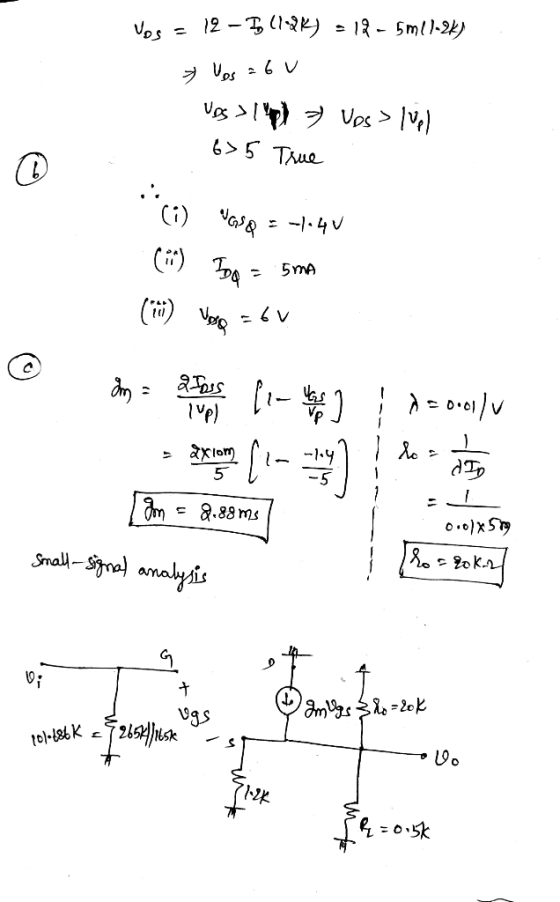
#4 The accompanying circuit shows a 4-resistor biased JFET transistor Determine the values of Rp and Rs so that the Q-point is equal to, VDsq 10 V and IDg 5 mA . For the JFET take IDss = 10 mA...
 #4
The accompanying circuit shows a 4-resistor biased JFET transistor Determine the values of Rp and Rs so that the Q-point is equal to, VDsq 10 V and IDg 5 mA . For the JFET take IDss = 10 mA, VP =-5 V and λ 0 . The circuit parameters are, R1-740 k, R2-22 1.85 ka, Rs-85 ㏀ and RL-3.5 ㏀. Take the power supply VDD 24 V 2- Vo R1 Vi R2 Signal generator 4-In reference to the circuit...
#4
The accompanying circuit shows a 4-resistor biased JFET transistor Determine the values of Rp and Rs so that the Q-point is equal to, VDsq 10 V and IDg 5 mA . For the JFET take IDss = 10 mA, VP =-5 V and λ 0 . The circuit parameters are, R1-740 k, R2-22 1.85 ka, Rs-85 ㏀ and RL-3.5 ㏀. Take the power supply VDD 24 V 2- Vo R1 Vi R2 Signal generator 4-In reference to the circuit...
Problem 3: Design Problem On Figure P3a, you have a Common Source (CS) n-channel MOSFET amplifier....
 Problem 3: Design Problem On Figure P3a, you have a Common Source (CS) n-channel MOSFET amplifier. Notice the absence of a source resistor Rsig and load resistor R. If we know how the present amplifier (the one on Figure P3a) behaves without Rsig and RL, we can infer its behaviors if Rsig and R were to be added. design the amplifier circuit on Figure P3a, i.e., you have to find appropriate values for RGj You are to RG,, RD, and...
 Vcc= 15 V Rc 2 kO R1 10 kO Vo C1 R2=5 kQ Vs RE= 2 kQ Figure 1.1 [Rajah 1.1) SECTION A Bakagian A Question 1 Soalan 1 State THREE (3) operating regions in Bipolar Junction Transistor (BJT) and (a) briefly explain. [Nyatakan TIGA (3) kawasan operasi untuk transistor simpang dwikutub (BJT) dan jelaskan.] (3 Marks/Markah) (b) Based on the Figure 1.1, given B 100 and VBE (ON) 0.7 V. [Berdasarkan Rajah 1.1, diberi B 100 dan Vas (ON...
 Vcc= 15 V Rc 2 kO R1 10 kO Vo C1 R2=5 kQ Vs RE= 2 kQ Figure 1.1 [Rajah 1.1) SECTION A Bakagian A Question 1 Soalan 1 State THREE (3) operating regions in Bipolar Junction Transistor (BJT) and (a) briefly explain. [Nyatakan TIGA (3) kawasan operasi untuk transistor simpang dwikutub (BJT) dan jelaskan.] (3 Marks/Markah) (b) Based on the Figure 1.1, given B 100 and VBE (ON) 0.7 V. [Berdasarkan Rajah 1.1, diberi B 100 dan Vas (ON...
 0.2500 62 5 + 20 +18 V Given a complex circuit in Figure Q1. This complex circuit is to be viewed in a simpler form of Thevenin and Norton equivalent circuits a) Dengan menggunakan analisis nod, cari voltan Thevenin, Vrh di terminal a dan b. By applying Nodal analysis, find Thevenin voltage, Vru al terminal a and b. (4 markah/marks) b) Sekiranya terminal a dan b dibiarkan bersambung, tentukan nilai semasa arus yang melalui terminal tersebut, iaitu Isc. Berikutan itu,...
 A motor is given in Figure 1 with the terminal voltage of the motor is 320 V, armature resistance of 2 2, series field resistance of 3 2, and KC value of 0.248. Sebuah motor diberi dalam Rajah 1 dengun voltan pangkalan pada motor sebanyak 320 V, rintangan angker adalah 2 S rintangan madan sesiri adalah 3 Q, dan nilai KC sebanyak 0.248. Figure 1 Rajah I a) Calculate the speed of the motor in Figure 1 when the armature...
 UwJTOWIU (5 Marks / Markah) (b) Obtain the v(t) in Figure 3(a) using Fourier Transform if vy(t) = " u(t) V and is(t) = 28(t) A. "ul V dan (Dapatkan vt) di dalam Rajah 3(a) menggunakan jelmaan Fourier jika v.() - 1:(t) = 28(1) A.) (6 Marks / Markah) vo(t) 100 § 17+ vt) is(t) 28 1t) A Figure 2(a) fRajak 2(a)] yurtz The transfer function of a circuit is [Rangkap pindah untuk satu litar adalah m2 +12 H@=oja+2) If...
 URGENT
The NMOS in the shown figure has Vt = 0.8V, kn = 5 mA/V2, and VA = 40 V. The circuit also has Vdd = 5V, VSS = -5V, RG = RLD = 1 M2, and RLS = 0 A. [3 marks] Neglecting the channel length modulation effect, find the value of Rs so that the NMOS operates in saturation with Ip = 0.4 mA B. [2 marks] Neglecting the channel length modulation effect, find the largest possible value...
URGENT
The NMOS in the shown figure has Vt = 0.8V, kn = 5 mA/V2, and VA = 40 V. The circuit also has Vdd = 5V, VSS = -5V, RG = RLD = 1 M2, and RLS = 0 A. [3 marks] Neglecting the channel length modulation effect, find the value of Rs so that the NMOS operates in saturation with Ip = 0.4 mA B. [2 marks] Neglecting the channel length modulation effect, find the largest possible value...
 #4
The accompanying circuit shows a 4-resistor biased JFET transistor Determine the values of Rp and Rs so that the Q-point is equal to, VDsq 10 V and IDg 5 mA . For the JFET take IDss = 10 mA, VP =-5 V and λ 0 . The circuit parameters are, R1-740 k, R2-22 1.85 ka, Rs-85 ㏀ and RL-3.5 ㏀. Take the power supply VDD 24 V 2- Vo R1 Vi R2 Signal generator 4-In reference to the circuit...
#4
The accompanying circuit shows a 4-resistor biased JFET transistor Determine the values of Rp and Rs so that the Q-point is equal to, VDsq 10 V and IDg 5 mA . For the JFET take IDss = 10 mA, VP =-5 V and λ 0 . The circuit parameters are, R1-740 k, R2-22 1.85 ka, Rs-85 ㏀ and RL-3.5 ㏀. Take the power supply VDD 24 V 2- Vo R1 Vi R2 Signal generator 4-In reference to the circuit...
 Problem 3: Design Problem On Figure P3a, you have a Common Source (CS) n-channel MOSFET amplifier. Notice the absence of a source resistor Rsig and load resistor R. If we know how the present amplifier (the one on Figure P3a) behaves without Rsig and RL, we can infer its behaviors if Rsig and R were to be added. design the amplifier circuit on Figure P3a, i.e., you have to find appropriate values for RGj You are to RG,, RD, and...
Most questions answered within 3 hours.
-
Explain how you might use E. coli bacteria to produce human
growth hormone using the following:...
asked 20 seconds from now -
WHAT IS THE EFFEKT OF ADD K2CO3 TO ( METHANOL OG WATER)?
asked 13 minutes ago -
Calculate the cell potential, the equilibrium constant, and the
free-energy change for: Ca(s)+Mn2+(aq)(1M)⇌Ca2+(aq)(1M)+Mn(s) given
the following...
asked 11 minutes ago -
Determine the pH at the equivalence (stoichiometric) point in
the titration of 48 mL of 0.28...
asked 11 minutes ago -
11. In CPM/PERT, an activity that is on the critical path
A. has equal values for...
asked 18 minutes ago -
Using C++ :
A Pascals triangle row is constructed by looking at the previous
row and...
asked 35 minutes ago -
With what speed will the fastest photoelectrons be emitted from
a surface whose threshold wavelength is...
asked 34 minutes ago -
The following slope distances and differences in elevations
between the tape ends were recorded for a...
asked 36 minutes ago -
1. Assuming random walk markets and normally distributed
returns, if a one day VaR on an...
asked 45 minutes ago -
(a) With a variable life insurance policy, the rate of return on
the investment (the death...
asked 55 minutes ago -
By applying what you know about Grignard reagents and the
mechanism by which benzoic acid is...
asked 1 hour ago -
For thermoplastics, explain the effects of increasing of each of
the following properties on a polymer’s...
asked 1 hour ago