
Homework Answers
Please UPVOTE for my explanation. Thanks you.
Add Answer to:
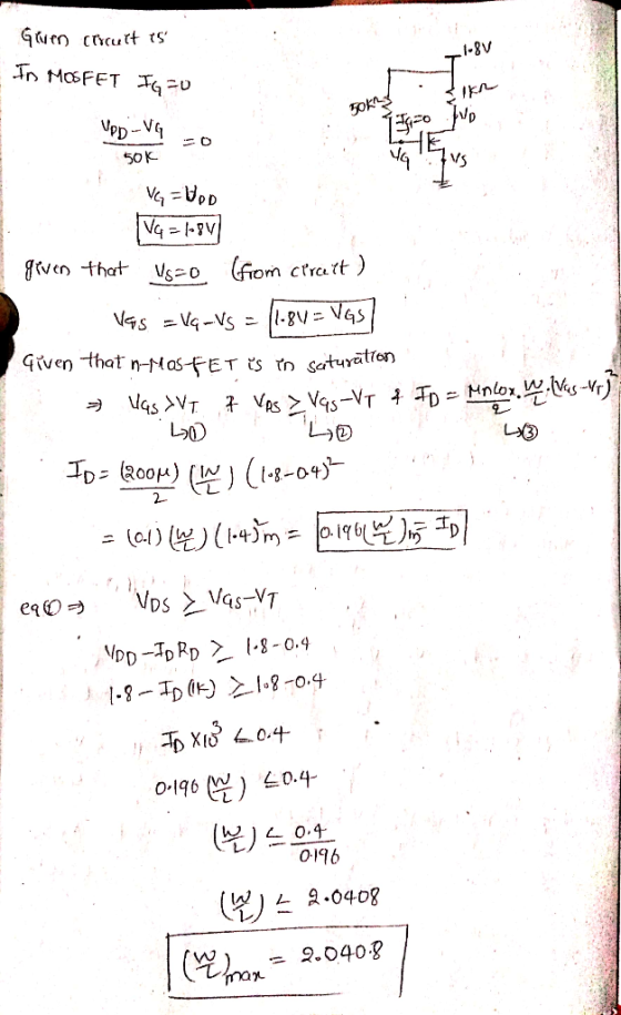
A5. For the circuit shown in Figure QA5, calculate the maximum allowable value of W/L to...
1. For the the SRAM cell in the figure below Find the Maximum allowable W/L for...
 1. For the the SRAM cell in the figure below Find the Maximum allowable W/L for the access transistor of the SRAM cell in the figure below so that in a read operation, the voltage at Q and do not change by more than IV,I. Assume that the SRAM is abricated in a o.18um technology for which Voo- 1.8V, VoVp-.5 and (w/y),-1.5 Determine the read delay At when (w/L)s. 1.5. Let μ.c.300μΑ/V. And CB-2pF and the sense Amplifier requires a...
A4. Design the circuit of Figure QA4 for a drain current of 1 mA. If W/L...
 A4. Design the circuit of Figure QA4 for a drain current of 1 mA. If W/L = 20/0.18, unCox = 100 A/V2, V1 = 0.6 V compute R1 and R2 such that the input impedance is at least 20 ka. VDD 1.8V 5000 R1 Q1 R2 Figure QA4 [4 marks]
4. Design the circuit of Figure 4 so that the transistor operates in saturation with ID0.5mAand V3V. Let the enhancement-type PMOS transistor have VV and k, (w/L)-1m4/V2. Assume λ-Ο What is the...
 4. Design the circuit of Figure 4 so that the transistor operates in saturation with ID0.5mAand V3V. Let the enhancement-type PMOS transistor have VV and k, (w/L)-1m4/V2. Assume λ-Ο What is the largest value that RD can have while maintaining saturation-region operation? VDD-+5 V o-0.5mA RG2 RG2 RD Figure 4
4. Design the circuit of Figure 4 so that the transistor operates in saturation with ID0.5mAand V3V. Let the enhancement-type PMOS transistor have VV and k, (w/L)-1m4/V2. Assume λ-Ο What...
4. Design the circuit of Figure 4 so that the transistor operates in saturation with ID0.5mAand V3V. Let the enhancement-type PMOS transistor have VV and k, (w/L)-1m4/V2. Assume λ-Ο What is the largest value that RD can have while maintaining saturation-region operation? VDD-+5 V o-0.5mA RG2 RG2 RD Figure 4
4. Design the circuit of Figure 4 so that the transistor operates in saturation with ID0.5mAand V3V. Let the enhancement-type PMOS transistor have VV and k, (w/L)-1m4/V2. Assume λ-Ο What...
URGENT The NMOS in the shown figure has Vt = 0.8V, kn = 5 mA/V2, and...
 URGENT
The NMOS in the shown figure has Vt = 0.8V, kn = 5 mA/V2, and VA = 40 V. The circuit also has Vdd = 5V, VSS = -5V, RG = RLD = 1 M2, and RLS = 0 A. [3 marks] Neglecting the channel length modulation effect, find the value of Rs so that the NMOS operates in saturation with Ip = 0.4 mA B. [2 marks] Neglecting the channel length modulation effect, find the largest possible value...
URGENT
The NMOS in the shown figure has Vt = 0.8V, kn = 5 mA/V2, and VA = 40 V. The circuit also has Vdd = 5V, VSS = -5V, RG = RLD = 1 M2, and RLS = 0 A. [3 marks] Neglecting the channel length modulation effect, find the value of Rs so that the NMOS operates in saturation with Ip = 0.4 mA B. [2 marks] Neglecting the channel length modulation effect, find the largest possible value...
TYU 16.5 Consider the NMOS logic circuit in Figure 16.18. Assume transistor parameters of kn = 10...
 need TYU 16.6
TYU 16.5 Consider the NMOS logic circuit in Figure 16.18. Assume transistor parameters of kn = 100 μ A/ V, and VT = 0.4 V. Assume all driver transistors are identical. Neglect the body effect. (a) If (W/L)L = 0.5, determine (W/L) for the drivers such that VOL(max) = 80μ V. Assume logic 1 input voltages are 2.1 V. 68 Part 3 Digital Electronics VDD = 5 V 0 MDA C DA B DC Figure 16.18 Figure...
need TYU 16.6
TYU 16.5 Consider the NMOS logic circuit in Figure 16.18. Assume transistor parameters of kn = 100 μ A/ V, and VT = 0.4 V. Assume all driver transistors are identical. Neglect the body effect. (a) If (W/L)L = 0.5, determine (W/L) for the drivers such that VOL(max) = 80μ V. Assume logic 1 input voltages are 2.1 V. 68 Part 3 Digital Electronics VDD = 5 V 0 MDA C DA B DC Figure 16.18 Figure...
Q5. Consider the circuit in Fig.1 (right). Assume 9m, 9o, VT, W, L, Mn, and Cox...
 Q5. Consider the circuit in Fig.1 (right). Assume 9m, 9o, VT, W, L, Mn, and Cox of the transistor are knwon and isolation capacitors are sufficiently large. Assume the transistor operates in saturation. (1) Find input resistance Rin (5 marks). (2) Find output resistance Rout (5 marks). (3) Find voltage gain v./vs (10 marks). (Q4). Right - MOSFET amplifier (Q5).
For the MOSFET bias circuit shown, what value of Rd in kilohms is needed to allow the maximum possible peak- to-peak signal swing on the drain without clipping? Use Vdd- 7V, Vss-7V, Vg-1.6V, Rs 9.1kQ...
 For the MOSFET bias circuit shown, what value of Rd in kilohms is needed to allow the maximum possible peak- to-peak signal swing on the drain without clipping? Use Vdd- 7V, Vss-7V, Vg-1.6V, Rs 9.1kQ, Vt-0.6V, [Vovl - [Vgsl 0.42. (Remember that (Von IVtl) Neglect the effect of channel-length modulation and body effect. (Hint: Be sure to keep the MOSFET in saturation!) V. M1 VD RD Answer: The correct answer is: 9.6
For the MOSFET bias circuit shown, what value...
For the MOSFET bias circuit shown, what value of Rd in kilohms is needed to allow the maximum possible peak- to-peak signal swing on the drain without clipping? Use Vdd- 7V, Vss-7V, Vg-1.6V, Rs 9.1kQ, Vt-0.6V, [Vovl - [Vgsl 0.42. (Remember that (Von IVtl) Neglect the effect of channel-length modulation and body effect. (Hint: Be sure to keep the MOSFET in saturation!) V. M1 VD RD Answer: The correct answer is: 9.6
For the MOSFET bias circuit shown, what value...
6.(14) For the nMOSFET circuit below, you want to operate the nMOSFET in saturation region with...
 6.(14) For the nMOSFET circuit below, you want to operate the nMOSFET in saturation region with ld-0.1 ma and Vd-0.3 volts. (a) What value of Rd and Rs will accomplish that? (b) Validate your computations that the nMOSFET is in saturation mode. Given Vt (threshold voltage) = 0.5 volt, unCox-400uamp/V squared, L= 0.4 um, w=5um. N DS
Problem 5: 13 pts The circuit shown below is called a current mirror. Essentially the output curr...
 Note: VDD = VSS = 5V, not VDD = -VSS = 5V
Problem 5: 13 pts The circuit shown below is called a current mirror. Essentially the output current Ip2 is multiples of the input current Ip1. Both transistors have the same VT = 1V. Transistor Q2 has k2 that is five times ki (transistor Q1 constant). Let iD2 ID1 02 V. (a) Find the value of R that makes the output current Ip2 0.5mA (assume Q2 is in SAT)....
Note: VDD = VSS = 5V, not VDD = -VSS = 5V
Problem 5: 13 pts The circuit shown below is called a current mirror. Essentially the output current Ip2 is multiples of the input current Ip1. Both transistors have the same VT = 1V. Transistor Q2 has k2 that is five times ki (transistor Q1 constant). Let iD2 ID1 02 V. (a) Find the value of R that makes the output current Ip2 0.5mA (assume Q2 is in SAT)....
Q #4: (6 marks). For the following circuit, all the transistors are biased in saturation region w...
 Q #4: (6 marks). For the following circuit, all the transistors are biased in saturation region with identical length and width of 1μm and 6.5μm, respectively. It is g 200μΑν-2, Wal Calculate the small signal parameters gm and ro for Q1. What is the value of voltage gain (Av)? iven that, VDD=5V, Vt= 1V, μ.co,- sor and 'REF-0.5mA. Draw the small signal circuit of the following amplifier. VDD es 02 REP ei Vo
Q #4: (6 marks). For the following...
Q #4: (6 marks). For the following circuit, all the transistors are biased in saturation region with identical length and width of 1μm and 6.5μm, respectively. It is g 200μΑν-2, Wal Calculate the small signal parameters gm and ro for Q1. What is the value of voltage gain (Av)? iven that, VDD=5V, Vt= 1V, μ.co,- sor and 'REF-0.5mA. Draw the small signal circuit of the following amplifier. VDD es 02 REP ei Vo
Q #4: (6 marks). For the following...
 1. For the the SRAM cell in the figure below Find the Maximum allowable W/L for the access transistor of the SRAM cell in the figure below so that in a read operation, the voltage at Q and do not change by more than IV,I. Assume that the SRAM is abricated in a o.18um technology for which Voo- 1.8V, VoVp-.5 and (w/y),-1.5 Determine the read delay At when (w/L)s. 1.5. Let μ.c.300μΑ/V. And CB-2pF and the sense Amplifier requires a...
 A4. Design the circuit of Figure QA4 for a drain current of 1 mA. If W/L = 20/0.18, unCox = 100 A/V2, V1 = 0.6 V compute R1 and R2 such that the input impedance is at least 20 ka. VDD 1.8V 5000 R1 Q1 R2 Figure QA4 [4 marks]
 4. Design the circuit of Figure 4 so that the transistor operates in saturation with ID0.5mAand V3V. Let the enhancement-type PMOS transistor have VV and k, (w/L)-1m4/V2. Assume λ-Ο What is the largest value that RD can have while maintaining saturation-region operation? VDD-+5 V o-0.5mA RG2 RG2 RD Figure 4
4. Design the circuit of Figure 4 so that the transistor operates in saturation with ID0.5mAand V3V. Let the enhancement-type PMOS transistor have VV and k, (w/L)-1m4/V2. Assume λ-Ο What...
4. Design the circuit of Figure 4 so that the transistor operates in saturation with ID0.5mAand V3V. Let the enhancement-type PMOS transistor have VV and k, (w/L)-1m4/V2. Assume λ-Ο What is the largest value that RD can have while maintaining saturation-region operation? VDD-+5 V o-0.5mA RG2 RG2 RD Figure 4
4. Design the circuit of Figure 4 so that the transistor operates in saturation with ID0.5mAand V3V. Let the enhancement-type PMOS transistor have VV and k, (w/L)-1m4/V2. Assume λ-Ο What...
 URGENT
The NMOS in the shown figure has Vt = 0.8V, kn = 5 mA/V2, and VA = 40 V. The circuit also has Vdd = 5V, VSS = -5V, RG = RLD = 1 M2, and RLS = 0 A. [3 marks] Neglecting the channel length modulation effect, find the value of Rs so that the NMOS operates in saturation with Ip = 0.4 mA B. [2 marks] Neglecting the channel length modulation effect, find the largest possible value...
URGENT
The NMOS in the shown figure has Vt = 0.8V, kn = 5 mA/V2, and VA = 40 V. The circuit also has Vdd = 5V, VSS = -5V, RG = RLD = 1 M2, and RLS = 0 A. [3 marks] Neglecting the channel length modulation effect, find the value of Rs so that the NMOS operates in saturation with Ip = 0.4 mA B. [2 marks] Neglecting the channel length modulation effect, find the largest possible value...
 need TYU 16.6
TYU 16.5 Consider the NMOS logic circuit in Figure 16.18. Assume transistor parameters of kn = 100 μ A/ V, and VT = 0.4 V. Assume all driver transistors are identical. Neglect the body effect. (a) If (W/L)L = 0.5, determine (W/L) for the drivers such that VOL(max) = 80μ V. Assume logic 1 input voltages are 2.1 V. 68 Part 3 Digital Electronics VDD = 5 V 0 MDA C DA B DC Figure 16.18 Figure...
need TYU 16.6
TYU 16.5 Consider the NMOS logic circuit in Figure 16.18. Assume transistor parameters of kn = 100 μ A/ V, and VT = 0.4 V. Assume all driver transistors are identical. Neglect the body effect. (a) If (W/L)L = 0.5, determine (W/L) for the drivers such that VOL(max) = 80μ V. Assume logic 1 input voltages are 2.1 V. 68 Part 3 Digital Electronics VDD = 5 V 0 MDA C DA B DC Figure 16.18 Figure...
 Q5. Consider the circuit in Fig.1 (right). Assume 9m, 9o, VT, W, L, Mn, and Cox of the transistor are knwon and isolation capacitors are sufficiently large. Assume the transistor operates in saturation. (1) Find input resistance Rin (5 marks). (2) Find output resistance Rout (5 marks). (3) Find voltage gain v./vs (10 marks). (Q4). Right - MOSFET amplifier (Q5).
 For the MOSFET bias circuit shown, what value of Rd in kilohms is needed to allow the maximum possible peak- to-peak signal swing on the drain without clipping? Use Vdd- 7V, Vss-7V, Vg-1.6V, Rs 9.1kQ, Vt-0.6V, [Vovl - [Vgsl 0.42. (Remember that (Von IVtl) Neglect the effect of channel-length modulation and body effect. (Hint: Be sure to keep the MOSFET in saturation!) V. M1 VD RD Answer: The correct answer is: 9.6
For the MOSFET bias circuit shown, what value...
For the MOSFET bias circuit shown, what value of Rd in kilohms is needed to allow the maximum possible peak- to-peak signal swing on the drain without clipping? Use Vdd- 7V, Vss-7V, Vg-1.6V, Rs 9.1kQ, Vt-0.6V, [Vovl - [Vgsl 0.42. (Remember that (Von IVtl) Neglect the effect of channel-length modulation and body effect. (Hint: Be sure to keep the MOSFET in saturation!) V. M1 VD RD Answer: The correct answer is: 9.6
For the MOSFET bias circuit shown, what value...
 6.(14) For the nMOSFET circuit below, you want to operate the nMOSFET in saturation region with ld-0.1 ma and Vd-0.3 volts. (a) What value of Rd and Rs will accomplish that? (b) Validate your computations that the nMOSFET is in saturation mode. Given Vt (threshold voltage) = 0.5 volt, unCox-400uamp/V squared, L= 0.4 um, w=5um. N DS
 Note: VDD = VSS = 5V, not VDD = -VSS = 5V
Problem 5: 13 pts The circuit shown below is called a current mirror. Essentially the output current Ip2 is multiples of the input current Ip1. Both transistors have the same VT = 1V. Transistor Q2 has k2 that is five times ki (transistor Q1 constant). Let iD2 ID1 02 V. (a) Find the value of R that makes the output current Ip2 0.5mA (assume Q2 is in SAT)....
Note: VDD = VSS = 5V, not VDD = -VSS = 5V
Problem 5: 13 pts The circuit shown below is called a current mirror. Essentially the output current Ip2 is multiples of the input current Ip1. Both transistors have the same VT = 1V. Transistor Q2 has k2 that is five times ki (transistor Q1 constant). Let iD2 ID1 02 V. (a) Find the value of R that makes the output current Ip2 0.5mA (assume Q2 is in SAT)....
 Q #4: (6 marks). For the following circuit, all the transistors are biased in saturation region with identical length and width of 1μm and 6.5μm, respectively. It is g 200μΑν-2, Wal Calculate the small signal parameters gm and ro for Q1. What is the value of voltage gain (Av)? iven that, VDD=5V, Vt= 1V, μ.co,- sor and 'REF-0.5mA. Draw the small signal circuit of the following amplifier. VDD es 02 REP ei Vo
Q #4: (6 marks). For the following...
Q #4: (6 marks). For the following circuit, all the transistors are biased in saturation region with identical length and width of 1μm and 6.5μm, respectively. It is g 200μΑν-2, Wal Calculate the small signal parameters gm and ro for Q1. What is the value of voltage gain (Av)? iven that, VDD=5V, Vt= 1V, μ.co,- sor and 'REF-0.5mA. Draw the small signal circuit of the following amplifier. VDD es 02 REP ei Vo
Q #4: (6 marks). For the following...
Most questions answered within 3 hours.
-
For this problem, carry at least four digits after the decimal
in your calculations. Answers may...
asked 2 hours ago -
Ask a user for three positive integer numbers. Use an input
validation loop to make sure...
asked 2 hours ago -
The most primitive form of data from data analysis perspective
is a. nominal scale b. ordinal...
asked 2 hours ago -
The number of vacancies in some hypothetical metal increases by
a factor of 5 when the...
asked 2 hours ago -
The fiduciary duty that is predicated on the concept that a
board of directors and officers...
asked 2 hours ago -
Sustainable Growth Rate Last year Umbrellas Unlimited
Corporation had an ROE of 17.3% and a dividend...
asked 3 hours ago -
Write a MATLAB program to do the following:
Receive 5 input values and store them into...
asked 3 hours ago -
Which one of the following aqueous solutions would you expect to
have the largest conductance: (a)...
asked 3 hours ago -
(Intermediate Macroeconomics)
2.The aggregate supply function be ys=2000+P, and the aggregate
demand function be yD=2400-P。Find the...
asked 3 hours ago -
I am having a really difficult time developing a strong thesis
for this question....... To what...
asked 3 hours ago -
There are n street lights in a line. In order to conserve
energy, the city decides...
asked 3 hours ago -
Cellular growth and repair require a cell to go through the cell
cycle. Like all biological...
asked 3 hours ago