![Question#2: [ABET S.O. D] (6marks) Design control unit that generates a signal from a 4 unit-sized inverter. The signal must](http://img.homeworklib.com/questions/0fc76280-2303-11eb-a3fa-a798ca4e020d.png?x-oss-process=image/resize,w_560)
![Question#3: [ABET ILO; C] (4mrks) Consider a process in which pMOS transistors have three times the effective resistance as n](http://img.homeworklib.com/questions/104ca3e0-2303-11eb-b4be-d5b6c8efd42a.png?x-oss-process=image/resize,w_560)
Homework Answers
Answer #1


Initial Drivers +64 + +64 +64 +64 + + + Datapath Loads N: 1 2 3 f 64 8 4 D: 65 18 15 - 4 2.8 15.3
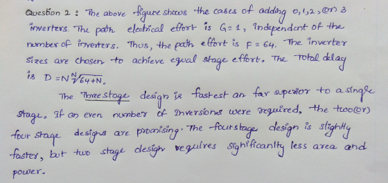
Question 2 : The above figure shows the cases of adding 0,12,01 3 inverters. The path electrical effort is G=1, independent of the number of inverters. Thus, the path elfort is f= 64. The inverter Sizes are chosen to achieve equal stage effort, the total delay is D=N/64+N. - The Three stage design is fastest an fear superior to a single stage. If an even number of Inversions were required, the two on four stage designs are pomising. The fourstage design is slightly faster, but two stage design requires significanity less area and power.
Question #3: Now since the effective resistance of pmos transistor is 3 times as much as amos transistor the sizing of the NAND and NOR gates will be different first for a NAND gate recall that the pull down network was two series of nmos transistor so in order to have the same fall resistance as the inverter the width have to be twice the whit width. Now we sees NAND gates. MANDRig = 5/4 NOR 29 = 74. The Inverter has 3it en ratio and 4 units of capacitance. The NAND has a 3:2 ratio and 5 units of capacitance, while the NOR has a 6:1 ratio and yunits of capacitance,
Know the answer?
Add Answer to:
Question#2: [ABET S.O. D] (6marks) Design control unit that generates a signal from a 4 unit-sized...
Not the answer you're looking for?
Ask your own homework help question.
Our experts will answer your question WITHIN MINUTES for Free.
Similar Homework Help Questions
CMOS Design Styles Quiz Problem 1: a) What is the typical "topology" for pMOS and nMOS...
CMOS Design Styles Quiz Problem 1: a) What is the typical "topology" for pMOS and nMOS in digital circuitry? -pMOS Vdd to Vout, nMOS Vout to Gnd -nMOS Vdd to Vout, pMOS Vout to Gnd -pMOS Vdd to Gnd, nMOS Vin to Vout -Only use xMOS -Both transistors Vin to Vout b) How do you implement nMOS in AND functions? -series connected, with increased widths -Parallel connected, with standard widths -Series connected with half the widths -Parallel connected, alternating large...
ADVERTISEMENT
Need Online Homework Help?
Ask
a QuestionGet Answers For Free
Most questions answered within 3 hours.
Most questions answered within 3 hours.
ADVERTISEMENT
ADVERTISEMENT
Active Questions
-
With a $16 Trillion national ebt, and projected annual budget
eficits in excess of $1 Trillion...
asked 2 minutes ago -
A machine shop owner wishes to assign each of three machinists
(labeled 1, 2, and 3)...
asked 16 minutes ago -
Regarding language development, which of the following
statements is FALSE?
Babies are able to cry from...
asked 16 minutes ago -
A couple of small ice cubes at 0 °C are added to glass of warm
water...
asked 14 minutes ago -
Slow 'n Steady, Inc., has a stock price of $30, will pay a
dividend next year...
asked 18 minutes ago -
During the current financial year, the owner of Omega
Enterprises withdrew supplies of $2,000 for personal...
asked 14 minutes ago -
PLEASE SHOW MATH CALCULATION(formulas)it has to be done on excel
P12-4 Last year (2016), Richter Condos...
asked 22 minutes ago -
A 0.25μF capacitor is charged to 50 V . It is then connected in
series with...
asked 38 minutes ago -
Calculate the current, I, through the batteries for:
- a 2-bulb parallel circuit
- How does...
asked 40 minutes ago -
Choose the sentence that uses correct punctuation.
1a. The prefatory parts of a report include the...
asked 46 minutes ago -
For the element arsenic, which one of the following sets of
quantum numbers could not apply...
asked 55 minutes ago -
Compare and contrast the architectures of 3 types of ADCs:
Flash, SAR, and pipelined. Use the...
asked 56 minutes ago
ADVERTISEMENT