equilibrium

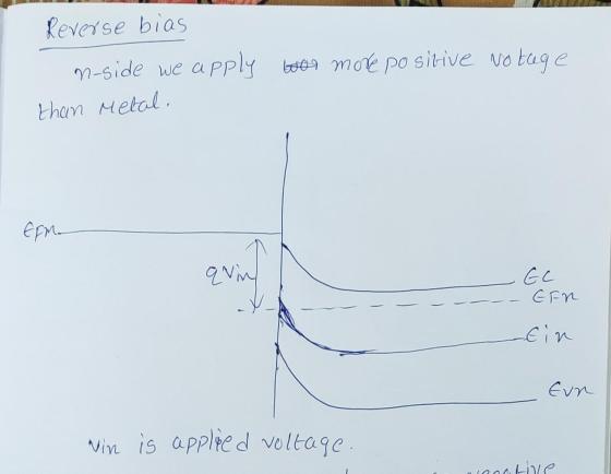
Draw the equilibrium and reverse-biased band diagram (indicate Ec, Ev, EF, E0, Ei) for- metal/semiconductor junction with the following specifications: [(3+3)M +(3+3)M]
Metal work function = 5 eV
Band-gap = 1.0 eV
Electron Affinity = 4.5 eV
Fermi Potential = 0.4 eV
Case 2
Metal work function = 5 eV
Band-gap = 1.0 eV
Electron Affinity = 4.5 eV
Fermi Potential = -0.4 eV
Acceptor Concentration = 1016 cm-3
Homework Answers


Problem 5. We want to make a Schottky diode on one surface of an n-type semiconductor, and an ohm...
 Problem 5. We want to make a Schottky diode on one surface of an n-type semiconductor, and an ohmic contact on the other side. The electron affinity is 5 eV, bandgap is 1.5 eV, and the Fermi potential (the difference between the Fermi level Ef and the intrinsic level Ei) is 0.25 eV d the values of the work functions of the two metals be? (Give your answer as greater than or less than certain values.) Sketch the band diagram...
equilibrium
 For a Metal-Insulator-Semiconductor (n-type) structure-1. Draw the C-V characteristics in high frequency and low frequency 2. Draw the band diagram (indicate Ec, Ev, EF, E0, Ei) from metal to semiconductor for:A) Accumulation RegionB) Depletion RegionC) Inversion Region3. Draw the charge density from metal to semiconductor for:A) Accumulation RegionB) Inversion Region
Draw the band diagram (the relative positions of conduction band edge EC, valence band edge Ev,...
 Draw the band diagram (the relative positions of conduction band
edge EC, valence band edge Ev, Fermi level EF) for the four
following cases. Clearly note EC −EF, EF −EV, Ei −EF, EG = EC −EV.
Ei is the intrinsic Fermi level. Take NC=NV =1025 m−3, EG=1.1 eV,
ni=1.5×10¹⁶ m−3, kT=0.026 eV.
(Q1.1) p-type, NA=5×10²³ m−3.
(Q1.2) p-type, NA=5×10²¹ m−3.
(Q1.3) n-type, ND=5×10²³ m−3.
(Q1.4) n-type, ND=5×10²¹ m−3.
Q2 Draw the band diagram (the relative positions of conduction band edge...
Draw the band diagram (the relative positions of conduction band
edge EC, valence band edge Ev, Fermi level EF) for the four
following cases. Clearly note EC −EF, EF −EV, Ei −EF, EG = EC −EV.
Ei is the intrinsic Fermi level. Take NC=NV =1025 m−3, EG=1.1 eV,
ni=1.5×10¹⁶ m−3, kT=0.026 eV.
(Q1.1) p-type, NA=5×10²³ m−3.
(Q1.2) p-type, NA=5×10²¹ m−3.
(Q1.3) n-type, ND=5×10²³ m−3.
(Q1.4) n-type, ND=5×10²¹ m−3.
Q2 Draw the band diagram (the relative positions of conduction band edge...
1. a. Find the main error in each of the band diagrams shown below. For all...
 1. a. Find the main error in each of the band diagrams shown below. For all of the band diagrams Ny 1019/cm3, Ne- 1019/cm3, ni = 3 x 10⁸/cm". E,-1.25 eV, T = 300 K. Ef Ef EFi Main error: Main error: Main error: Main error: Consider a semiconductor sample with the following characteristics: EG 1.25 eV, T 300 K, Nd 5 x 101*/cm3, Na 1014/cm3, N.-1019/cm3, N.-1019/cm3, ni-3 × 10⁸/cm3. Assume complete ionization b. Find the equilibrium electron and...
Draw the energy band diagram at equilibrium for the p+ /n/p semiconductor heterostructure (p+ indicates a...
Draw the energy band diagram at equilibrium for the p+ /n/p semiconductor heterostructure (p+ indicates a p-type semiconductor which is heavily doped, i.e., more heavily doped than p). You should indicate Ec (conduction band), Ev (valence band), Ei (intrinsic Fermi level), and Ef (Fermi level) throughout the device structure. show your work (i.e., you should start from the diagram of individual material pieces). State any reason for your drawing.
An ideal metal-semiconductor (M-S) junction is formed on the n-type Si semiconductor that is uniformly doped...
 An ideal metal-semiconductor (M-S) junction is formed on the n-type Si semiconductor that is uniformly doped with a donor impurity (phosphorus) concentration of 1016 cm. The metal work function is 4.5 eV, and the Si electron affinity is 4 eV. Assuming that this M-S junction is at 300K, give your best answers to the following questions. (50 points) (a) At thermal equilibrium, draw the energy band diagram including meaningful parameters (energy barriers, energy levels, depletion width, etc.). (b) Calculate the...
(2) In a semiconductor with an energy gap Eg between the valence and the conduction bands we can take Ef (the Fermi ene...
 (2) In a semiconductor with an energy gap Eg between the valence and the conduction bands we can take Ef (the Fermi energy) to be halfway between the bands (see figure below): Conduction band Energy gap Eg Valence band Semiconductor a. Show that for a typical semiconductor or insulator at room temperature the Fermi- Dirac factor is approximately equal to exp(-E 2kBT). (Typical Eg for semi-conductors ranges from about 0.5eV to 6eV at T-293K.) b. In heavily doped n-type silicon,...
7. Find the position of the intrinsic Fermi level with respect to Emidgap for silicon, germanium,...
 7. Find the position of the intrinsic Fermi level with respect to Emidgap for silicon, germanium, gallium arsenide, and indium arsenide. Use the effective density of states values from problem 5. 8. a. Draw a band diagram for silicon doped 107/cmp-type and label the band gap and the position of the Fermi level. b. Draw a band diagram for gallium arsenide doped 10/cmn-type and label the band gap and the position of the Fermi level. c. Draw a band diagram...
6. A silicon wafer is doped with donor atoms, N-5x0 cm(bonus question) (a) Determine (Ec-EF), (EF...
 6. A silicon wafer is doped with donor atoms, N-5x0 cm(bonus question) (a) Determine (Ec-EF), (EF-Ev), (Ep-E) at 300 K. Assume all the donor atoms are ionized. (b) Plot the position of Fermi level (EF) in the bandgap as a function of temperature for 300 Ts700 K. In this temperature range, it can be assumed that all the donor atoms are ionized. (c) Plot the position of Fermi level (Er) in the bandgap as acceptor atoms are added (N.- 104,...
A) Show that the chemical potential in an intrinsic semiconductor lies in the middle of the gap a...
a) Show that the chemical potential in an intrinsic semiconductor lies in the middle of the gap at low temperature. (b) Explain how the chemical potential varies with temperature if the semiconductor is doped with (i) donors (ii) acceptors. (c) A direct-gap semiconductor is doped to produce a density of 1023electrons/m3. Calculate the hole density at room temperature given that the gap is 1.0 eV, and the effective mass of carriers in the conduction and valence band are 0.25 and...
 Problem 5. We want to make a Schottky diode on one surface of an n-type semiconductor, and an ohmic contact on the other side. The electron affinity is 5 eV, bandgap is 1.5 eV, and the Fermi potential (the difference between the Fermi level Ef and the intrinsic level Ei) is 0.25 eV d the values of the work functions of the two metals be? (Give your answer as greater than or less than certain values.) Sketch the band diagram...
 Draw the band diagram (the relative positions of conduction band
edge EC, valence band edge Ev, Fermi level EF) for the four
following cases. Clearly note EC −EF, EF −EV, Ei −EF, EG = EC −EV.
Ei is the intrinsic Fermi level. Take NC=NV =1025 m−3, EG=1.1 eV,
ni=1.5×10¹⁶ m−3, kT=0.026 eV.
(Q1.1) p-type, NA=5×10²³ m−3.
(Q1.2) p-type, NA=5×10²¹ m−3.
(Q1.3) n-type, ND=5×10²³ m−3.
(Q1.4) n-type, ND=5×10²¹ m−3.
Q2 Draw the band diagram (the relative positions of conduction band edge...
Draw the band diagram (the relative positions of conduction band
edge EC, valence band edge Ev, Fermi level EF) for the four
following cases. Clearly note EC −EF, EF −EV, Ei −EF, EG = EC −EV.
Ei is the intrinsic Fermi level. Take NC=NV =1025 m−3, EG=1.1 eV,
ni=1.5×10¹⁶ m−3, kT=0.026 eV.
(Q1.1) p-type, NA=5×10²³ m−3.
(Q1.2) p-type, NA=5×10²¹ m−3.
(Q1.3) n-type, ND=5×10²³ m−3.
(Q1.4) n-type, ND=5×10²¹ m−3.
Q2 Draw the band diagram (the relative positions of conduction band edge...
 1. a. Find the main error in each of the band diagrams shown below. For all of the band diagrams Ny 1019/cm3, Ne- 1019/cm3, ni = 3 x 10⁸/cm". E,-1.25 eV, T = 300 K. Ef Ef EFi Main error: Main error: Main error: Main error: Consider a semiconductor sample with the following characteristics: EG 1.25 eV, T 300 K, Nd 5 x 101*/cm3, Na 1014/cm3, N.-1019/cm3, N.-1019/cm3, ni-3 × 10⁸/cm3. Assume complete ionization b. Find the equilibrium electron and...
 An ideal metal-semiconductor (M-S) junction is formed on the n-type Si semiconductor that is uniformly doped with a donor impurity (phosphorus) concentration of 1016 cm. The metal work function is 4.5 eV, and the Si electron affinity is 4 eV. Assuming that this M-S junction is at 300K, give your best answers to the following questions. (50 points) (a) At thermal equilibrium, draw the energy band diagram including meaningful parameters (energy barriers, energy levels, depletion width, etc.). (b) Calculate the...
 (2) In a semiconductor with an energy gap Eg between the valence and the conduction bands we can take Ef (the Fermi energy) to be halfway between the bands (see figure below): Conduction band Energy gap Eg Valence band Semiconductor a. Show that for a typical semiconductor or insulator at room temperature the Fermi- Dirac factor is approximately equal to exp(-E 2kBT). (Typical Eg for semi-conductors ranges from about 0.5eV to 6eV at T-293K.) b. In heavily doped n-type silicon,...
 7. Find the position of the intrinsic Fermi level with respect to Emidgap for silicon, germanium, gallium arsenide, and indium arsenide. Use the effective density of states values from problem 5. 8. a. Draw a band diagram for silicon doped 107/cmp-type and label the band gap and the position of the Fermi level. b. Draw a band diagram for gallium arsenide doped 10/cmn-type and label the band gap and the position of the Fermi level. c. Draw a band diagram...
 6. A silicon wafer is doped with donor atoms, N-5x0 cm(bonus question) (a) Determine (Ec-EF), (EF-Ev), (Ep-E) at 300 K. Assume all the donor atoms are ionized. (b) Plot the position of Fermi level (EF) in the bandgap as a function of temperature for 300 Ts700 K. In this temperature range, it can be assumed that all the donor atoms are ionized. (c) Plot the position of Fermi level (Er) in the bandgap as acceptor atoms are added (N.- 104,...
Most questions answered within 3 hours.
-
An MNE is this kind of industry when competition in one country
is essentially independent of...
asked 1 hour ago -
. For this set of questions, determine what
proportion of a normal distribution is located betweeneach...
asked 2 hours ago -
A college student is employed as a door-to-door newspaper
salesman. Historical data suggests that the student...
asked 3 hours ago -
MATLAB HW 11 problem using Switch Case and Input commands
Write a script file that calculates...
asked 2 hours ago -
Considering gravitational time dilation, calculate the time that
passes in Earth’s surface while 1 hour passes...
asked 3 hours ago -
Minitab Problem: Take the Lake Hume June rainfall data and find
use the processes outlined in...
asked 4 hours ago -
X Company is trying to decide whether to continue using old
equipment to make Product A...
asked 4 hours ago -
IN PYTHON ONLY !! Program 2: Re-work
program #5 (WeeklyHours) from the previous assignment such that...
asked 4 hours ago -
The average length of time between arrivals at a turnpike
toll-booth is 26 seconds. What is...
asked 6 hours ago -
(a) A piston at 6.1 atm contains a gas that occupies a volume of
3.5 L....
asked 7 hours ago -
Please answer true or false. Words
cannot be changed or added in to make it true...
asked 7 hours ago -
An empty test tube weighs 15.923 grams. Then,
MgCl2•6H2O is added into the test tube. After...
asked 7 hours ago