
Homework Answers
Add Answer to:
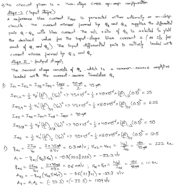
Q5: Consider the following Multistage amplifier with kn' = 160 uA/V?, kp' = 40 A/V, and...
3. Consider the following multistage amplifier. The current source values are 1, -2mA, I, - 1mA,...
 3. Consider the following multistage amplifier. The current source values are 1, -2mA, I, - 1mA, and 1 - 1mA. Also, Voo - Vss - 6V. +VDD (a) If the DC voltage at the output is OV, find all DC currents at the drains of all transistors. Also, find the DC voltages at the drain, gate, and source terminals for all transistors (you can put the values directly on the figure). Use k.(W/L) - k.(W/L) = 2mA/V. And Vin -...
An analogue amplifier circuit is shown in Figure 1 below. VDD Q5 15V JL - Vout...
 An analogue amplifier circuit is shown in Figure 1 below. VDD Q5 15V JL - Vout Irer RI Vina JET T7T Figure 1 Integrated amplifier circuit. Circuit Data: Vpp = 15 V, IREF = I1 = I2 = 1.0 mA Transistor Data: Q1: NMOS, un Cox = 80 A/V?, W/L = 100 um/0.8 um, Vtn = 0.8 V, L = 0.10 um/V Q2: NPN BJT, B = 100, Vbe = 0.7 V, VA = 150 V Q3, Q4: NMOS, un...
pleaseee solve quickly it s urgent!!!!! EEN 311-Electronic Circuits ll (3 eredíįs)-Final Exam fferential amplifier biased with a basic current source rollowing parameters: Voo-Va 12 V. RD 8 ka, a...
 pleaseee solve quickly it s urgent!!!!!
EEN 311-Electronic Circuits ll (3 eredíįs)-Final Exam fferential amplifier biased with a basic current source rollowing parameters: Voo-Va 12 V. RD 8 ka, and 5. (20 points) Consider the di The circuit has the param Vi - 650 mv, Vov 50 mV, and R 10 k2. The transistors are matched and have: Va=80 V 几 Von Ro &K 오, DGI + VDD REF Q4 THE DE CEER Vss Determine: a) the reference current IREF...
pleaseee solve quickly it s urgent!!!!!
EEN 311-Electronic Circuits ll (3 eredíįs)-Final Exam fferential amplifier biased with a basic current source rollowing parameters: Voo-Va 12 V. RD 8 ka, and 5. (20 points) Consider the di The circuit has the param Vi - 650 mv, Vov 50 mV, and R 10 k2. The transistors are matched and have: Va=80 V 几 Von Ro &K 오, DGI + VDD REF Q4 THE DE CEER Vss Determine: a) the reference current IREF...
5) Consider the Cascode amplifier shown below. For the NMOS transistors, kn 0.2 mA/V2, Vr,-0.5 V,...
 5) Consider the Cascode amplifier shown below. For the NMOS transistors, kn 0.2 mA/V2, Vr,-0.5 V, (W/L)-(W/L)2-5. VDD-GV and IBIAs= 1.0 mA. a) Assuming λ-0 for all transistors, find the required DC gate- source voltages of M1 and M2 (VGsı and VGs2, respectively) BIAS VD out b) Again assuming 0 M2 for all transistors, what is the minimum DC value of VouT for which the amplifier works in high-gain regime? (W/L)2 in M1 For parts c)-f), Assume -0.01 for all...
29. Identify the type of third stage amplifier: a) inverting amplifier; b) differential amplifier with passi load; c) differential amplifier with current mirror load; d) emitter follower; e...
 29. Identify the type of third stage amplifier: a) inverting amplifier; b) differential amplifier with passi load; c) differential amplifier with current mirror load; d) emitter follower; e) none of above; 30. The Vsg of Q5 should be: a)-1V, b)-0.85% c) 0.65% d)0.85% env 31. To obtain IREF-30μΑ , the value of R should be: a)250ohm; b)25Kohm; c)250Kohm; d)2.5Mohm; e 5Mohm. network is composed by 4 identical phase shifter. The phase shift of each phase shifter in degree should be...
QUESTION 2: (20 MARKS) +5 V X2 71 QA X2 ×10 5 V Figure Q2.1 The...
 QUESTION 2: (20 MARKS) +5 V X2 71 QA X2 ×10 5 V Figure Q2.1 The circuit shown in Figure Q2.1, is a multistage amplifier with a differential input stage It uses a folded cascode involving transistor Q3. Note that transistor Q5 operates in class B mode and is off at the quiescent point, while Q4 is ON at the quiescent point with QD sinking its bias current. All transistors have Vad-0.7V, VA-200 V, and β-100 a) Perform a dc...
-o +V cc А A 11 Q3 Q4 AES Q5 U U2 Q Q2 26. 5...
 -o +V cc А A 11 Q3 Q4 AES Q5 U U2 Q Q2 26. 5 AV Q1 А VO 5A V 012 A RL 27 IREF Q. Q10 08 A A 5 A --VEE Figure 16.44 Complete bipolar operational amplifier. Part 2) Use B (beta) = 100 and VA = 100 V for all transistors when calculating gains. However, assume ideal current mirrors - i.e., don't worry about ß or VA corrections when calculating the currents. Also assume a...
please answer all spring 2019 Name 19. Gain Margin (dB) is: e1OdByb) 15dBa c) 20 d8;...
 please answer all
spring 2019 Name 19. Gain Margin (dB) is: e1OdByb) 15dBa c) 20 d8; d) 35dB; e) 45d8 20. Phase margin (degree) is close to: a) 0; b) 45pe90) 135) e) 180 21. A MOSFET transistor gm 2m5, Cgs 2pF, Ced 0.5pF, its cut-off frequency, ft, is close to: a) 100 b) 300MHz ) 60OMH)1GHe) SGH 22. The cut-off frequency of a BIT with gm-40m5, r pi-2.5Kohm, r o-20Kohm, c mu 1pF and c pi is close to:...
please answer all
spring 2019 Name 19. Gain Margin (dB) is: e1OdByb) 15dBa c) 20 d8; d) 35dB; e) 45d8 20. Phase margin (degree) is close to: a) 0; b) 45pe90) 135) e) 180 21. A MOSFET transistor gm 2m5, Cgs 2pF, Ced 0.5pF, its cut-off frequency, ft, is close to: a) 100 b) 300MHz ) 60OMH)1GHe) SGH 22. The cut-off frequency of a BIT with gm-40m5, r pi-2.5Kohm, r o-20Kohm, c mu 1pF and c pi is close to:...
 3. Consider the following multistage amplifier. The current source values are 1, -2mA, I, - 1mA, and 1 - 1mA. Also, Voo - Vss - 6V. +VDD (a) If the DC voltage at the output is OV, find all DC currents at the drains of all transistors. Also, find the DC voltages at the drain, gate, and source terminals for all transistors (you can put the values directly on the figure). Use k.(W/L) - k.(W/L) = 2mA/V. And Vin -...
 An analogue amplifier circuit is shown in Figure 1 below. VDD Q5 15V JL - Vout Irer RI Vina JET T7T Figure 1 Integrated amplifier circuit. Circuit Data: Vpp = 15 V, IREF = I1 = I2 = 1.0 mA Transistor Data: Q1: NMOS, un Cox = 80 A/V?, W/L = 100 um/0.8 um, Vtn = 0.8 V, L = 0.10 um/V Q2: NPN BJT, B = 100, Vbe = 0.7 V, VA = 150 V Q3, Q4: NMOS, un...
 pleaseee solve quickly it s urgent!!!!!
EEN 311-Electronic Circuits ll (3 eredíįs)-Final Exam fferential amplifier biased with a basic current source rollowing parameters: Voo-Va 12 V. RD 8 ka, and 5. (20 points) Consider the di The circuit has the param Vi - 650 mv, Vov 50 mV, and R 10 k2. The transistors are matched and have: Va=80 V 几 Von Ro &K 오, DGI + VDD REF Q4 THE DE CEER Vss Determine: a) the reference current IREF...
pleaseee solve quickly it s urgent!!!!!
EEN 311-Electronic Circuits ll (3 eredíįs)-Final Exam fferential amplifier biased with a basic current source rollowing parameters: Voo-Va 12 V. RD 8 ka, and 5. (20 points) Consider the di The circuit has the param Vi - 650 mv, Vov 50 mV, and R 10 k2. The transistors are matched and have: Va=80 V 几 Von Ro &K 오, DGI + VDD REF Q4 THE DE CEER Vss Determine: a) the reference current IREF...
 5) Consider the Cascode amplifier shown below. For the NMOS transistors, kn 0.2 mA/V2, Vr,-0.5 V, (W/L)-(W/L)2-5. VDD-GV and IBIAs= 1.0 mA. a) Assuming λ-0 for all transistors, find the required DC gate- source voltages of M1 and M2 (VGsı and VGs2, respectively) BIAS VD out b) Again assuming 0 M2 for all transistors, what is the minimum DC value of VouT for which the amplifier works in high-gain regime? (W/L)2 in M1 For parts c)-f), Assume -0.01 for all...
 29. Identify the type of third stage amplifier: a) inverting amplifier; b) differential amplifier with passi load; c) differential amplifier with current mirror load; d) emitter follower; e) none of above; 30. The Vsg of Q5 should be: a)-1V, b)-0.85% c) 0.65% d)0.85% env 31. To obtain IREF-30μΑ , the value of R should be: a)250ohm; b)25Kohm; c)250Kohm; d)2.5Mohm; e 5Mohm. network is composed by 4 identical phase shifter. The phase shift of each phase shifter in degree should be...
 QUESTION 2: (20 MARKS) +5 V X2 71 QA X2 ×10 5 V Figure Q2.1 The circuit shown in Figure Q2.1, is a multistage amplifier with a differential input stage It uses a folded cascode involving transistor Q3. Note that transistor Q5 operates in class B mode and is off at the quiescent point, while Q4 is ON at the quiescent point with QD sinking its bias current. All transistors have Vad-0.7V, VA-200 V, and β-100 a) Perform a dc...
 -o +V cc А A 11 Q3 Q4 AES Q5 U U2 Q Q2 26. 5 AV Q1 А VO 5A V 012 A RL 27 IREF Q. Q10 08 A A 5 A --VEE Figure 16.44 Complete bipolar operational amplifier. Part 2) Use B (beta) = 100 and VA = 100 V for all transistors when calculating gains. However, assume ideal current mirrors - i.e., don't worry about ß or VA corrections when calculating the currents. Also assume a...
 please answer all
spring 2019 Name 19. Gain Margin (dB) is: e1OdByb) 15dBa c) 20 d8; d) 35dB; e) 45d8 20. Phase margin (degree) is close to: a) 0; b) 45pe90) 135) e) 180 21. A MOSFET transistor gm 2m5, Cgs 2pF, Ced 0.5pF, its cut-off frequency, ft, is close to: a) 100 b) 300MHz ) 60OMH)1GHe) SGH 22. The cut-off frequency of a BIT with gm-40m5, r pi-2.5Kohm, r o-20Kohm, c mu 1pF and c pi is close to:...
please answer all
spring 2019 Name 19. Gain Margin (dB) is: e1OdByb) 15dBa c) 20 d8; d) 35dB; e) 45d8 20. Phase margin (degree) is close to: a) 0; b) 45pe90) 135) e) 180 21. A MOSFET transistor gm 2m5, Cgs 2pF, Ced 0.5pF, its cut-off frequency, ft, is close to: a) 100 b) 300MHz ) 60OMH)1GHe) SGH 22. The cut-off frequency of a BIT with gm-40m5, r pi-2.5Kohm, r o-20Kohm, c mu 1pF and c pi is close to:...
Most questions answered within 3 hours.
-
Problem: Patient Fees C++
You are to write a program that computes a patient’s bill for...
asked 1 hour ago -
In a population of interest, we know that, 77% drink coffee, and
23% drink tea. Assume...
asked 1 hour ago -
Given that f(x) = e-(x-1) for x > 1, determine the following
probabilities:
a) P(X <...
asked 1 hour ago -
A mechanic pushes a 2.60 ✕ 103-kg car from rest to a speed of v,
doing...
asked 1 hour ago -
International information systems result in all of the following
except:
A. improved quality of information flow....
asked 1 hour ago -
The president of the retailer Prime Products has just approached
the company’s bank with a request...
asked 1 hour ago -
If the carrying amount is $200,000 and recoverable amount is
$205000, the impairment amount is:
Select...
asked 1 hour ago -
The correlation is inappropriate as a measure of association
between two quantitative variables (you may select...
asked 1 hour ago -
USE THE DATA IN THE TABLE BELOW TO ANSWER QUESTIONS 19 – 24
(Assume all account...
asked 1 hour ago -
Mahaley, Inc., manufactures and sells two products: Product Q9
and Product F0. Data concerning the expected...
asked 2 hours ago -
To measure the current through one branch of a parallel circuit,
the meter is connected ________....
asked 2 hours ago -
a)
The following table shows the profile, by the math section of
the SAT Reasoning Test,...
asked 2 hours ago