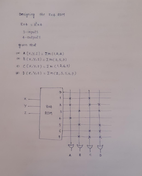
Tabulate the truth table for an 8x4 ROM that implements the Boolean functions. (a) A(X, Y,...
Tabulate the truth table for an 8x4 ROM that implements the
Boolean functions.
(a) A(X, Y, Z) = Σm(1, 2, 4)
(b) B(X, Y, Z) = Σm(3, 5, 7)
(c) C(X, Y, Z) = Σm(1, 2, 6, 7)
(d) D(X, Y, Z) = Σm(2, 3, 5, 6, 7)
Homework Answers
Having any doubts please comment below. Thank you.

Add Answer to:
Tabulate the truth table for an 8x4 ROM that implements the
Boolean functions.
(a) A(X, Y,...
Q3) (10 points] Tabulate the truth table of an 8x4 ROM that implements the following functions:...
 Q3) (10 points] Tabulate the truth table of an 8x4 ROM that implements the following functions: F. (A,B,C) = A'B + AC F1 (A,B,C) = A'B'C' +C F2 (A,B,C) = A'B' + AB F3 (A,B,C) = AB + AC + BC F1 F2 F3 Address Fo ABC 000 001 010 011 100 101 110 111
1. Read Only Memory Design a ROM that implements the following four Boolean functions: A(x,y,z)-2...
 1. Read Only Memory Design a ROM that implements the following four Boolean functions: A(x,y,z)-2m(2, 3, 4, 5) B(x,y,z)-2m(0, 1, 2, 6) C(x,y,z) -2m(0, 3, 4, 5, 7) D(x,y,z) -2m(3, 5, 6) Make sure you are using an appropriately sized decoder, all lines are clear, and all "connections" are clearly marked.
1. Read Only Memory Design a ROM that implements the following four Boolean functions: A(x,y,z)-2m(2, 3, 4, 5) B(x,y,z)-2m(0, 1, 2, 6) C(x,y,z) -2m(0, 3, 4, 5, 7) D(x,y,z)...
1. Read Only Memory Design a ROM that implements the following four Boolean functions: A(x,y,z)-2m(2, 3, 4, 5) B(x,y,z)-2m(0, 1, 2, 6) C(x,y,z) -2m(0, 3, 4, 5, 7) D(x,y,z) -2m(3, 5, 6) Make sure you are using an appropriately sized decoder, all lines are clear, and all "connections" are clearly marked.
1. Read Only Memory Design a ROM that implements the following four Boolean functions: A(x,y,z)-2m(2, 3, 4, 5) B(x,y,z)-2m(0, 1, 2, 6) C(x,y,z) -2m(0, 3, 4, 5, 7) D(x,y,z)...
Derive the truth table for the following Boolean functions: F(x,y,z) = x'y'z' + x'yz + xy'z'...
Derive the truth table for the following Boolean functions: F(x,y,z) = x'y'z' + x'yz + xy'z' + xyz
We are interested in designing a circuit that implements the following three Boolean functions: 3. h(x,y,z)=Σm(1,4,6)...
 We are interested in designing a circuit that implements the following three Boolean functions: 3. h(x,y,z)=Σm(1,4,6) f1x,y,z)- > m(1,4,6) y-m35) (x,y, z) Σ m (2,4,6,7) 左 You are supposed to implement the circuit with a decoder constructed with NAND gates (a) [12pt] Start by drawing the block diagram of a NAND-based decoder with three inputs (x,y,z), labelling all the outputs with their corresponding Boolean functions (b) [8pt) Using a new block diagram of the NAND-based decoder, implement the circuit using...
Design a PLA that implements the followingthree boolean function A(w,x,y,z) = ?m(4, 5, 7, 12, 13,...
Design a PLA that implements the followingthree boolean function A(w,x,y,z) = ?m(4, 5, 7, 12, 13, 15) B(w,x,y,z) = ?m(0, 1, 4, 5, 8, 9, 11, 12, 13, 15) C(w,x,y,z) = ?m(0, 1, 2, 3, 6, 7, 8, 9, 10, 11, 14) a) Use Karnaugh Maps to optimal each function and its complement. b)Select the three optimal functions to use in the PLA. C)Optimize the equation(s) using Karnaugh Map(s). d.Draw the circuit (Don't forget the clock).
Having the next Boolean functions: F1(x,y,z)-П (1, 3, 5) . F2(x,y,z)-Σ (0, 2, 4, 5) . 1. Make one...
 Computer architecture
Having the next Boolean functions: F1(x,y,z)-П (1, 3, 5) . F2(x,y,z)-Σ (0, 2, 4, 5) . 1. Make one logic gate design circuit, using AND, OR and NOT logic gates (20 points). 2. Design two 4-to-1 selectors, one for each Boolean function (20 points) 3. Design one 3-to-8 decoder to solve both Boolean functions (20 points) 4. Design a 8x2 ROM to solve both Boolean functions (20 points) 5. Design a 3x5x2 PLA to solve both Boolean functions...
Computer architecture
Having the next Boolean functions: F1(x,y,z)-П (1, 3, 5) . F2(x,y,z)-Σ (0, 2, 4, 5) . 1. Make one logic gate design circuit, using AND, OR and NOT logic gates (20 points). 2. Design two 4-to-1 selectors, one for each Boolean function (20 points) 3. Design one 3-to-8 decoder to solve both Boolean functions (20 points) 4. Design a 8x2 ROM to solve both Boolean functions (20 points) 5. Design a 3x5x2 PLA to solve both Boolean functions...
Given four-input Boolean functions, F1 (A,B,C,D) = Σm(4, 5, 10, 11, 12)
Given four-input Boolean functions, F1 (A,B,C,D) = Σm(4, 5, 10, 11, 12) F2 (A,B,C,D) = Σm(0, 1, 3, 4, 8, 11) F3 (A,B,C,D) = Σm(0, 4, 10, 12, 14) (a) Realize F1, F2 and F3 using a ROM. (b) Realize F1, F2 and F3 using a PLA of minimum size. Show the PLA table and location of switches.
Boolean Logic A. Show the truth table for this expression: X AND (Y XOR X) B....
Boolean Logic A. Show the truth table for this expression: X AND (Y XOR X) B. Show the truth table for this expression: Y OR (Y AND NOT X) C. Show the truth table for this expression: X NOR (Y NAND X) D. Draw a digital logic circuit for the expression used in 3A. E. Draw a digital logic circuit for the expression used in 3B. F. Draw a digital logic circuit for the expression used in 3C.
1. Find the Boolean expression of the truth table. Then simplify it and convert it into...
 1. Find the Boolean expression of the truth table. Then simplify it and convert it into the least amount of logic gates possible. AB Output 100 011 101 2. Find the POS form of the Boolean expressions below. Find the truth table and logic minimization method of it. Show its gate level implementation, and show the same gate level implementation using only NAND gates. A(X,Y,Z)= m(0,2,4,6) B(X,Y,2)={m(0,4,5) 3. Create a J-k Flip Flop using a D-Flip Flop. Show its truth...
For the following functions and using Boolean identities a) Simplify the given functions b) Construct the...
 For the following functions and using Boolean identities a) Simplify the given functions b) Construct the truth table for both of them showing the output of the original function and the simplified one and compare the two outputs? c) Draw the logic circuits for both the original function and the simplified one? 1. FIX, Y, Z) = X'+Y' + XY'Z 2. F(X, Y, Z) = (X+Y)(X' +Y+Z)
 Q3) (10 points] Tabulate the truth table of an 8x4 ROM that implements the following functions: F. (A,B,C) = A'B + AC F1 (A,B,C) = A'B'C' +C F2 (A,B,C) = A'B' + AB F3 (A,B,C) = AB + AC + BC F1 F2 F3 Address Fo ABC 000 001 010 011 100 101 110 111
 1. Read Only Memory Design a ROM that implements the following four Boolean functions: A(x,y,z)-2m(2, 3, 4, 5) B(x,y,z)-2m(0, 1, 2, 6) C(x,y,z) -2m(0, 3, 4, 5, 7) D(x,y,z) -2m(3, 5, 6) Make sure you are using an appropriately sized decoder, all lines are clear, and all "connections" are clearly marked.
1. Read Only Memory Design a ROM that implements the following four Boolean functions: A(x,y,z)-2m(2, 3, 4, 5) B(x,y,z)-2m(0, 1, 2, 6) C(x,y,z) -2m(0, 3, 4, 5, 7) D(x,y,z)...
1. Read Only Memory Design a ROM that implements the following four Boolean functions: A(x,y,z)-2m(2, 3, 4, 5) B(x,y,z)-2m(0, 1, 2, 6) C(x,y,z) -2m(0, 3, 4, 5, 7) D(x,y,z) -2m(3, 5, 6) Make sure you are using an appropriately sized decoder, all lines are clear, and all "connections" are clearly marked.
1. Read Only Memory Design a ROM that implements the following four Boolean functions: A(x,y,z)-2m(2, 3, 4, 5) B(x,y,z)-2m(0, 1, 2, 6) C(x,y,z) -2m(0, 3, 4, 5, 7) D(x,y,z)...
 We are interested in designing a circuit that implements the following three Boolean functions: 3. h(x,y,z)=Σm(1,4,6) f1x,y,z)- > m(1,4,6) y-m35) (x,y, z) Σ m (2,4,6,7) 左 You are supposed to implement the circuit with a decoder constructed with NAND gates (a) [12pt] Start by drawing the block diagram of a NAND-based decoder with three inputs (x,y,z), labelling all the outputs with their corresponding Boolean functions (b) [8pt) Using a new block diagram of the NAND-based decoder, implement the circuit using...
 Computer architecture
Having the next Boolean functions: F1(x,y,z)-П (1, 3, 5) . F2(x,y,z)-Σ (0, 2, 4, 5) . 1. Make one logic gate design circuit, using AND, OR and NOT logic gates (20 points). 2. Design two 4-to-1 selectors, one for each Boolean function (20 points) 3. Design one 3-to-8 decoder to solve both Boolean functions (20 points) 4. Design a 8x2 ROM to solve both Boolean functions (20 points) 5. Design a 3x5x2 PLA to solve both Boolean functions...
Computer architecture
Having the next Boolean functions: F1(x,y,z)-П (1, 3, 5) . F2(x,y,z)-Σ (0, 2, 4, 5) . 1. Make one logic gate design circuit, using AND, OR and NOT logic gates (20 points). 2. Design two 4-to-1 selectors, one for each Boolean function (20 points) 3. Design one 3-to-8 decoder to solve both Boolean functions (20 points) 4. Design a 8x2 ROM to solve both Boolean functions (20 points) 5. Design a 3x5x2 PLA to solve both Boolean functions...
 1. Find the Boolean expression of the truth table. Then simplify it and convert it into the least amount of logic gates possible. AB Output 100 011 101 2. Find the POS form of the Boolean expressions below. Find the truth table and logic minimization method of it. Show its gate level implementation, and show the same gate level implementation using only NAND gates. A(X,Y,Z)= m(0,2,4,6) B(X,Y,2)={m(0,4,5) 3. Create a J-k Flip Flop using a D-Flip Flop. Show its truth...
 For the following functions and using Boolean identities a) Simplify the given functions b) Construct the truth table for both of them showing the output of the original function and the simplified one and compare the two outputs? c) Draw the logic circuits for both the original function and the simplified one? 1. FIX, Y, Z) = X'+Y' + XY'Z 2. F(X, Y, Z) = (X+Y)(X' +Y+Z)
Most questions answered within 3 hours.
-
Write the net ionic equation for the precipitation reaction that
occurs when aqueous solutions of potassium...
asked 7 minutes ago -
it
should be written in c++
Your program should take numbers from the user until the...
asked 13 minutes ago -
Buses are powered by chemical reactions. Define matter and the
four states of matter. What is...
asked 30 minutes ago -
Use conservation of energy to find the velocity of a free point
charge q1 at 22cm...
asked 38 minutes ago -
First, describe policies promoted by governments of the
political right to address economic globalization. Second, describe...
asked 55 minutes ago -
M2-9 Completing T-Accounts LO2-4
Following are the transactions of Dennen, Inc., for the month of
January....
asked 55 minutes ago -
Write a program using python that reads from values from a text
file and plots them...
asked 56 minutes ago -
Look up the density of
the metal of the object used in parts A and B...
asked 56 minutes ago -
Discuss strategic considerations that Amazon and NYC politicians
had. Analyze why the deal between Amazon and...
asked 59 minutes ago -
A combustion reaction is describes as a carbon source reacting
with oxygen and producing carbon dioxide...
asked 1 hour ago -
Buckminsterfullerence is a recently allotrope of carbon in which
carbon atoms form molecules of formula C_60,...
asked 1 hour ago -
Lower Equitorial and Upper Equitorial are the same except Lower
Equitorial has a larger capital stock....
asked 1 hour ago