


Homework Answers
We have to design the circuits for the comparator, circuit A and circuit B. From the given table in the question, the comparator checks if the input is greater than 9. That means if the input is greater than 9 the output z will be 1. Here the muxes have also been used. The output of mux depends on the select line. If the select line is 0 then the input at 0 port will be transmitted to the output, and if the select line is 1 the input at 1 will be transmitted to the output. The truth table of the comparator is given below. The inputs are V3, V2, V1 and V0. The output is z.

For ciruit A, the muxes take the output of circuit A when the input is greater than nine. This is because the output of the comparator is used as the select line for the muxes and the output of A is conected at the 1 port of the muxes. From the table given in the question we can see that for input greater than 9 the output of A is going to the 7 segment decoder. The circuit has three inputs V2, V1 and V0 and three outputs. The truth table for the circuit A is shown below. when input is 010 output should be 000 for getting 0 on the 7 segment display. Similarly when input is 011 output should be 001 for getting 1 on the 7 segment display. Accordingly the truth table is written.

For circuit B, the input is Z, the output of the comparator and the output is 7 bit for the 7 segment display. When input is 0 output should be zero and when input is 1 output should be 1 on the 7 segment display. The truth table for cicuit B is given below:
![Touth Table fore Circuit B input =z, output = di [6:0] = a b c d e fg » Common-anode < 7- Segment display. 3 active lows on.](http://img.homeworklib.com/questions/6dc37f50-77a0-11eb-9903-33591613cf02.png?x-oss-process=image/resize,w_560)
For finding SoP (sum of products) we have to take the product of inputs when output is one and OR eah product. For minimiization Karnaugh map is used. When don't cares come they are used only for reduction of ones and are not considered if they are associated with a one.
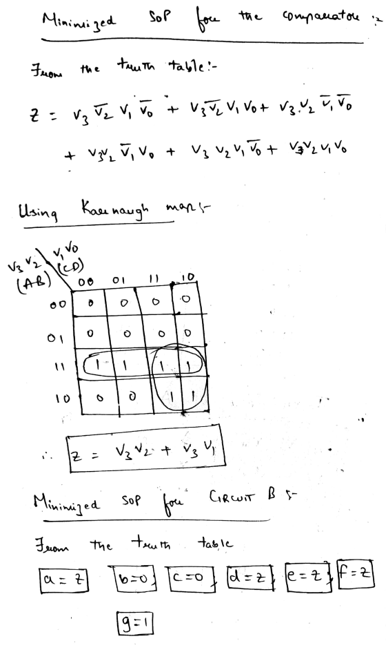

The schematic for the comparator, circuit A nad circuit B are shown below according to the minimized SoP expression:
![Schematic foce comparcaton A ist 2 = vs [w: +vo) ] Schematic Ciuenit As - Az = A, svi](http://img.homeworklib.com/questions/6feed650-77a0-11eb-842c-cf73bf4fc401.png?x-oss-process=image/resize,w_560)

Add Answer to:
Preparation (Pre-lab) Before coming to the first lab session, complete the following tasks: Generate a truth...
(a) Write a truth table. The input is 4-bit binary ABCD, A is MSB, D is...
 (a) Write a truth table. The input is 4-bit binary ABCD, A is
MSB, D is LSB. The output is also represented by x.
(b) Obtain an output expression in the form of a SOP.
(c) Use Boolean Algebra to design a circuit consisting of only
four inverters, four 3-input and gate, and one 4-input OR gate
using the simplified and simplified expression obtained in (b).
4-6. The Excess-3 coding system is a four-bit digital coding system for encoding all...
(a) Write a truth table. The input is 4-bit binary ABCD, A is
MSB, D is LSB. The output is also represented by x.
(b) Obtain an output expression in the form of a SOP.
(c) Use Boolean Algebra to design a circuit consisting of only
four inverters, four 3-input and gate, and one 4-input OR gate
using the simplified and simplified expression obtained in (b).
4-6. The Excess-3 coding system is a four-bit digital coding system for encoding all...
Objective: In this lab, we will learn how we can design sequential circuits using behavioral mode...
 Just need the code for the
random counter,Thanks
Objective: In this lab, we will learn how we can design sequential circuits using behavioral modelling, and implementing the design in FPGA. Problem: Design a random counter with the following counting sequence: Counting Sequence: 04 2 9 168573 Design Description: The counter has one clock (Clock), one reset (Reset), and one move left or right control signal (L/R) as input. The counter also has one 4bit output O and one 2bit output...
Just need the code for the
random counter,Thanks
Objective: In this lab, we will learn how we can design sequential circuits using behavioral modelling, and implementing the design in FPGA. Problem: Design a random counter with the following counting sequence: Counting Sequence: 04 2 9 168573 Design Description: The counter has one clock (Clock), one reset (Reset), and one move left or right control signal (L/R) as input. The counter also has one 4bit output O and one 2bit output...
from 6 to 1 and from 4 to 1 Draw the schematic diagram for the circuit...
 from 6 to 1 and from 4 to 1
Draw the schematic diagram for the circuit shown in Figure W1.1 using schematic capture software (refer Table 2). The drawing should include labels for DC supply and 1/O pin numbers as in the actual ic pin configuration (Refer AN2). W1.2 Instruction You are required to design and built a 1-digit decimal down counter from decimal value A to decimal valuie Ron a breadboard (refer ANI). Values of A and B will...
from 6 to 1 and from 4 to 1
Draw the schematic diagram for the circuit shown in Figure W1.1 using schematic capture software (refer Table 2). The drawing should include labels for DC supply and 1/O pin numbers as in the actual ic pin configuration (Refer AN2). W1.2 Instruction You are required to design and built a 1-digit decimal down counter from decimal value A to decimal valuie Ron a breadboard (refer ANI). Values of A and B will...
ECE 1552- Summer 2019 Homework 2: Solve all questions. HW is to be turned in as a PDF or word document on canvas. Show...
 ECE 1552- Summer 2019 Homework 2: Solve all questions. HW is to be turned in as a PDF or word document on canvas. Show all working. Answers provided should be typed or written CLEARLY 1: Find a function to detect an error in the representation of a decimal digit in BCD. In other words, write an equation with value 1 when the inputs are any one of the six unused bit combinations in the BCD code, and value 0 otherwise...
I need the tasks done. I'm unsure how to do it with a chart like that....
 I need the tasks done. I'm unsure how to do it with a
chart like that. thanks!
Lab Exercises: (1) You need to do a design and simulate (NI Multisim) for the logic circuit of a coffee vending machine. Your client, KappaCappuccino, student based coffee startup company, wants their vending machines to vend "buy-one-get-one free" coffee for some specific coffees. Table T 1 is the truth table for one of their vending machines. The coffees are numbered from 0 to...
I need the tasks done. I'm unsure how to do it with a
chart like that. thanks!
Lab Exercises: (1) You need to do a design and simulate (NI Multisim) for the logic circuit of a coffee vending machine. Your client, KappaCappuccino, student based coffee startup company, wants their vending machines to vend "buy-one-get-one free" coffee for some specific coffees. Table T 1 is the truth table for one of their vending machines. The coffees are numbered from 0 to...
please anwer all the part of this lab and please use multisim. Lab 4: Basic Logic...
 please anwer all the part of this lab and please use
multisim.
Lab 4: Basic Logic Gates and Multisim Tools Objectives: • Learn to use the Logic Converter in Multisim to generate truth tables, design circuits and simplify logic expressions. • Build logic circuits using basic TTL gates. Software and Materials: • Multisim One 7400 (quad 2-input NAND gate) IC chip Procedure: 1. Write a logic expression for the circuit below. Have your instructor check the expression. А B с...
please anwer all the part of this lab and please use
multisim.
Lab 4: Basic Logic Gates and Multisim Tools Objectives: • Learn to use the Logic Converter in Multisim to generate truth tables, design circuits and simplify logic expressions. • Build logic circuits using basic TTL gates. Software and Materials: • Multisim One 7400 (quad 2-input NAND gate) IC chip Procedure: 1. Write a logic expression for the circuit below. Have your instructor check the expression. А B с...
Pre-lab: Design and implement on the NEXYS board the following FSM circuit. There is one input...
 Pre-lab: Design and implement on the NEXYS board the following FSM circuit. There is one input called direction. If direction 1, the FSM will make the segments in one 7-segment display (will be referred to as the most significant digit, MSD) move in a clockwise direction around in a circle (i.e., turn on and off the segments in this order: segment a, b, c, d, e, f, a, b,...) and the segments in a neighboring 7-segment display (LSD) move in...
The place values for the eight binary digits used in IPv4 addressing are as follows: 128,...
The place values for the eight binary digits used in IPv4 addressing are as follows: 128, 64, 32, 16, 8, 4, 2, 1. Expand this range to include an additional four bits. Do this by recording the place values for 211, 210, 29, and 28. 1111 Express the decimal value 2001 in binary by placing 1s in the binary positions requiring the addition of the corresponding place value. Place 0s in the binary positions where the corresponding place value should...
i need help with a mips program to to covert roman numerals to real numbers Lab 4: Roman Numeral Conversion Part A: Due...
 i need help with a mips program to to covert roman numerals to
real numbers
Lab 4: Roman Numeral Conversion Part A: Due Sunday, 19 May 2019, 11:59 PM Due Friday, 24 May 2019, 11:59 PM Part B: Minimum Submission Requirements Ensure that your Lab4 folder contains the following files (note the capitalization convention): o Diagram.pdf o Lab4. asm O README.txt Commit and push your repository Lab Objective In this lab, you will develop a more detailed understanding of how...
i need help with a mips program to to covert roman numerals to
real numbers
Lab 4: Roman Numeral Conversion Part A: Due Sunday, 19 May 2019, 11:59 PM Due Friday, 24 May 2019, 11:59 PM Part B: Minimum Submission Requirements Ensure that your Lab4 folder contains the following files (note the capitalization convention): o Diagram.pdf o Lab4. asm O README.txt Commit and push your repository Lab Objective In this lab, you will develop a more detailed understanding of how...
 (a) Write a truth table. The input is 4-bit binary ABCD, A is
MSB, D is LSB. The output is also represented by x.
(b) Obtain an output expression in the form of a SOP.
(c) Use Boolean Algebra to design a circuit consisting of only
four inverters, four 3-input and gate, and one 4-input OR gate
using the simplified and simplified expression obtained in (b).
4-6. The Excess-3 coding system is a four-bit digital coding system for encoding all...
(a) Write a truth table. The input is 4-bit binary ABCD, A is
MSB, D is LSB. The output is also represented by x.
(b) Obtain an output expression in the form of a SOP.
(c) Use Boolean Algebra to design a circuit consisting of only
four inverters, four 3-input and gate, and one 4-input OR gate
using the simplified and simplified expression obtained in (b).
4-6. The Excess-3 coding system is a four-bit digital coding system for encoding all...
 Just need the code for the
random counter,Thanks
Objective: In this lab, we will learn how we can design sequential circuits using behavioral modelling, and implementing the design in FPGA. Problem: Design a random counter with the following counting sequence: Counting Sequence: 04 2 9 168573 Design Description: The counter has one clock (Clock), one reset (Reset), and one move left or right control signal (L/R) as input. The counter also has one 4bit output O and one 2bit output...
Just need the code for the
random counter,Thanks
Objective: In this lab, we will learn how we can design sequential circuits using behavioral modelling, and implementing the design in FPGA. Problem: Design a random counter with the following counting sequence: Counting Sequence: 04 2 9 168573 Design Description: The counter has one clock (Clock), one reset (Reset), and one move left or right control signal (L/R) as input. The counter also has one 4bit output O and one 2bit output...
 from 6 to 1 and from 4 to 1
Draw the schematic diagram for the circuit shown in Figure W1.1 using schematic capture software (refer Table 2). The drawing should include labels for DC supply and 1/O pin numbers as in the actual ic pin configuration (Refer AN2). W1.2 Instruction You are required to design and built a 1-digit decimal down counter from decimal value A to decimal valuie Ron a breadboard (refer ANI). Values of A and B will...
from 6 to 1 and from 4 to 1
Draw the schematic diagram for the circuit shown in Figure W1.1 using schematic capture software (refer Table 2). The drawing should include labels for DC supply and 1/O pin numbers as in the actual ic pin configuration (Refer AN2). W1.2 Instruction You are required to design and built a 1-digit decimal down counter from decimal value A to decimal valuie Ron a breadboard (refer ANI). Values of A and B will...
 ECE 1552- Summer 2019 Homework 2: Solve all questions. HW is to be turned in as a PDF or word document on canvas. Show all working. Answers provided should be typed or written CLEARLY 1: Find a function to detect an error in the representation of a decimal digit in BCD. In other words, write an equation with value 1 when the inputs are any one of the six unused bit combinations in the BCD code, and value 0 otherwise...
 I need the tasks done. I'm unsure how to do it with a
chart like that. thanks!
Lab Exercises: (1) You need to do a design and simulate (NI Multisim) for the logic circuit of a coffee vending machine. Your client, KappaCappuccino, student based coffee startup company, wants their vending machines to vend "buy-one-get-one free" coffee for some specific coffees. Table T 1 is the truth table for one of their vending machines. The coffees are numbered from 0 to...
I need the tasks done. I'm unsure how to do it with a
chart like that. thanks!
Lab Exercises: (1) You need to do a design and simulate (NI Multisim) for the logic circuit of a coffee vending machine. Your client, KappaCappuccino, student based coffee startup company, wants their vending machines to vend "buy-one-get-one free" coffee for some specific coffees. Table T 1 is the truth table for one of their vending machines. The coffees are numbered from 0 to...
 please anwer all the part of this lab and please use
multisim.
Lab 4: Basic Logic Gates and Multisim Tools Objectives: • Learn to use the Logic Converter in Multisim to generate truth tables, design circuits and simplify logic expressions. • Build logic circuits using basic TTL gates. Software and Materials: • Multisim One 7400 (quad 2-input NAND gate) IC chip Procedure: 1. Write a logic expression for the circuit below. Have your instructor check the expression. А B с...
please anwer all the part of this lab and please use
multisim.
Lab 4: Basic Logic Gates and Multisim Tools Objectives: • Learn to use the Logic Converter in Multisim to generate truth tables, design circuits and simplify logic expressions. • Build logic circuits using basic TTL gates. Software and Materials: • Multisim One 7400 (quad 2-input NAND gate) IC chip Procedure: 1. Write a logic expression for the circuit below. Have your instructor check the expression. А B с...
 Pre-lab: Design and implement on the NEXYS board the following FSM circuit. There is one input called direction. If direction 1, the FSM will make the segments in one 7-segment display (will be referred to as the most significant digit, MSD) move in a clockwise direction around in a circle (i.e., turn on and off the segments in this order: segment a, b, c, d, e, f, a, b,...) and the segments in a neighboring 7-segment display (LSD) move in...
 i need help with a mips program to to covert roman numerals to
real numbers
Lab 4: Roman Numeral Conversion Part A: Due Sunday, 19 May 2019, 11:59 PM Due Friday, 24 May 2019, 11:59 PM Part B: Minimum Submission Requirements Ensure that your Lab4 folder contains the following files (note the capitalization convention): o Diagram.pdf o Lab4. asm O README.txt Commit and push your repository Lab Objective In this lab, you will develop a more detailed understanding of how...
i need help with a mips program to to covert roman numerals to
real numbers
Lab 4: Roman Numeral Conversion Part A: Due Sunday, 19 May 2019, 11:59 PM Due Friday, 24 May 2019, 11:59 PM Part B: Minimum Submission Requirements Ensure that your Lab4 folder contains the following files (note the capitalization convention): o Diagram.pdf o Lab4. asm O README.txt Commit and push your repository Lab Objective In this lab, you will develop a more detailed understanding of how...
Most questions answered within 3 hours.
-
In C++
In this homework, you will be tasked with creating functions to
manipulate strings that...
asked 1 minute ago -
An isolated colony represents a pure culture. one rare occasions
, however , a colony can...
asked 16 minutes ago -
*****DO NOT ANSWER THIS QUESTION IF YOU DON'T
KNOW*******Rights and Duties of Auditors; Minimum 4000
words...
asked 1 hour ago -
The probability that Janie is wearing sunglasses is 1/4. The
probability that she is wearing sunglasses...
asked 1 hour ago -
Do you believe social media is more of a help or a hindrance in
controlling crises...
asked 1 hour ago -
Two long, parallel wires separated by 2.85 cm carry currents in
opposite directions. The current in...
asked 1 hour ago -
Question # 1. Develop a list of rehabilitation journals
that publish articles concerning career counseling for...
asked 1 hour ago -
Bryant Company has a factory machine with a book value of
$85,100 and a remaining useful...
asked 1 hour ago -
What is the default classification for federal tax purposes of a
U.S. eligible entity with one...
asked 2 hours ago -
1. How many grams would 4.0x10²¹ atoms of calcium
weigh?
2.. Calculate the percent oxygen in...
asked 1 hour ago -
Balance Equation
K2Cr2O7 + H2C2O4 2H2O 6 K[Cr(C2O4 )2 (H2O)2 ]2H2O + CO2 +
H2O
asked 2 hours ago -
Select a position in the clinical laboratory and write an
appropriate job description and corresponding work...
asked 2 hours ago