


Homework Answers
1)
The logic expression for the given circuit is


2)
![- -EX E Design 1 - Multisim - [Design1 *] File Edit View Place MCU Simulate Transfer Tools Reports Options Window Help 8 B é](http://img.homeworklib.com/questions/ac8b4e40-08d2-11eb-9a36-1d096b77ff6e.png?x-oss-process=image/resize,w_560)
3)
![- E Design 1 - Multisim - [Design1 *] Eile Edit View Place MCU Simulate Transfer Tools Reports Options Window Help -EX --- In](http://img.homeworklib.com/questions/ad0a7fe0-08d2-11eb-aa82-e34d70f836bd.png?x-oss-process=image/resize,w_560)
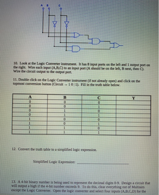
4)
Truth Table
| A | B | C | Y |
|---|---|---|---|
| 0 | 0 | 0 | 0 |
| 0 | 0 | 1 | 1 |
| 0 | 1 | 0 | 0 |
| 0 | 1 | 1 | 1 |
| 1 | 0 | 0 | 1 |
| 1 | 0 | 1 | 1 |
| 1 | 1 | 0 | 0 |
| 1 | 1 | 1 | 1 |
5)
Simplified Expression AB'+C
![G Design 1 - Multisim - [Design 1 *] Eile Edit View Place MCU Simulate Transfer Tools Reports Options Window Help GS --- In-U](http://img.homeworklib.com/questions/ad876d50-08d2-11eb-9b23-ad3c0ff20a94.png?x-oss-process=image/resize,w_560)
6)
using Only NAND gates
![- E Design 1 - Multisim - [Design1 *] File Edit View Place MCU Simulate Transfer Tools Reports Options Window Help -2X GA ---](http://img.homeworklib.com/questions/ae06e300-08d2-11eb-8d51-472bed924b92.png?x-oss-process=image/resize,w_560)
7)
Construction of the same circuit using 7400 Quad two input NAND Gate
![- Design2 - Multisim - [Design2 *] Eile Edit View Place MCU Simulate Transfer Tools Reports Options Window Help --- In-Use Li](http://img.homeworklib.com/questions/ae83b1a0-08d2-11eb-91bd-91b2d08dbde1.png?x-oss-process=image/resize,w_560)
8)
![- X Design3 - Multisim - [Design3 *] Eile Edit View Place MCU Simulate Transfer Tools Reports Options Window Help -6X GA ---](http://img.homeworklib.com/questions/af05af00-08d2-11eb-9ccf-dde915714f35.png?x-oss-process=image/resize,w_560)
9)10)
![- X Design3 - Multisim - [Design3 *] File Edit View Place MCU Simulate Transfer Tools Reports Options Window Help -6X --- In-](http://img.homeworklib.com/questions/af866950-08d2-11eb-b898-f38bae62b212.png?x-oss-process=image/resize,w_560)
11)
| A | B | C | Y |
| 0 | 0 | 0 | 1 |
| 0 | 0 | 1 | 0 |
| 0 | 1 | 0 | 0 |
| 0 | 1 | 1 | 1 |
| 1 | 0 | 0 | 1 |
| 1 | 0 | 1 | 1 |
| 1 | 1 | 0 | 0 |
| 1 | 1 | 1 | 1 |
12)
B'C'+AB'+BC
13)
AB+AC
14)
![- X Designs - Multisim - [Design5 *] Eile Edit View Place MCU Simulate Transfer Tools Reports Options Window Help -6X --- In-](http://img.homeworklib.com/questions/b00c1330-08d2-11eb-a7a9-772254d13239.png?x-oss-process=image/resize,w_560)
15)
![- Designs - Multisim - [Design5 *] Eile Edit View Place MCU Simulate Transfer Tools Reports Options Window Help -2X GA --- In](http://img.homeworklib.com/questions/b092d530-08d2-11eb-8bb3-5f0c2fcd827d.png?x-oss-process=image/resize,w_560)
Add Answer to:
please anwer all the part of this lab and please use
multisim.
Lab 4: Basic Logic...
AT&T 8:14 AM 100% < Back ECE204.Lab09-DataSheet.docx Гђ ECE 204 Lab 09 Basic Logic Gates Name: Na...
 AT&T 8:14 AM 100% < Back ECE204.Lab09-DataSheet.docx Гђ ECE 204 Lab 09 Basic Logic Gates Name: Name: Purpose: Replace this with a statement of purpose. Procedure A Digital input output test setup The digital circuits built throughout the rest of this lab will have the basic input and output setup as shown in Figure 1 Figure: Digital circuit input and output test setup The components for this setup include single throw dual pole switches and an LED. Figure 2 shows...
EE 210 Digital Logic Experiment 3 - Basic Combinational Logic: Adjacency Tester- Simulation only. In this...
 EE 210 Digital Logic Experiment 3 - Basic Combinational Logic: Adjacency Tester- Simulation only. In this experiment, the student will design and simulate a minimal AND, OR and INVERTER circuit, with 4 input variables A, B, C, and D, and output F, that will produce a logic 1 output whenever two adjacent input variables are 1s. In this context, the A and D variables are also treated as being adjacent variables. See the partially filled-in Truth Table below, for more...
digital logic & design questions 1. Find the output function of this circuit, X. B C...
 digital logic & design questions
1. Find the output function of this circuit, X. B C 2. Use k-map to simplify the function X to its minimum Sum Of Product (SOP Draw the logic circuit of the simplified function X using the 74LS54 And Or Invert (AOD chip. 3. 74LSS4 Problem#4: The logic circuit in (a) is implemented using a 7400 IC chip. The conections on is not working properly! the problem is in the IC connections or in the...
digital logic & design questions
1. Find the output function of this circuit, X. B C 2. Use k-map to simplify the function X to its minimum Sum Of Product (SOP Draw the logic circuit of the simplified function X using the 74LS54 And Or Invert (AOD chip. 3. 74LSS4 Problem#4: The logic circuit in (a) is implemented using a 7400 IC chip. The conections on is not working properly! the problem is in the IC connections or in the...
PRELIMINARY WORK 2: FUNCTIONS OF LOGIC GATES F (xyz) Figure 2.1-3-input-NAND Gate design by using just...
 PRELIMINARY WORK 2: FUNCTIONS OF LOGIC GATES F (xyz) Figure 2.1-3-input-NAND Gate design by using just 2-input-NAND Gates Figure 2.2- Design of function F-xy+x'z, by using just 2-input-NAND Gates Simulate the logic circuits that are given in figure 2.1 and figure 2.2. Simulations can be done in Proteus, P-Spice or any simulation program that you want to use. You can take screenshot of your design for print out. Please fill the table 2.1 according to your simulation results. Experiment results...
DESIGN SECTION Before the experiment, you are going to design a circuit which has 4 inputs...
DESIGN SECTION Before the experiment, you are going to design a circuit which has 4 inputs w, x, y, z and an output F. If 4-bits input value is “odd number which is higher than 4”, or “3-bits highest even number” or “4-bits highest even number”, the output function F will be equal to 1. Otherwise F=0. Each students have to design the circuit and have to do following steps own by own. You are going to; a) Fill the...
Design the logic circuit to display a 3 bit octal numbers from 0 to 7 on...
 Design the logic circuit to display a 3 bit octal numbers from 0 to 7 on a seven segment display shown below (for number 1 use segments b and c; for 6 include segment (a) Write the Truth Table with A, B. C representing the input bits (A is the MSB) and a, b, c, d, e, f and g representing the outputs to the seven segments. (b) Implement the circuit using a Programmable Logic Array (use simplified notation to...
3.4.1 Build and simulate the comparator circuit shown in Figure 3, in Multisim. The inputs A3,...
 3.4.1 Build and simulate the comparator circuit shown in Figure 3, in Multisim. The inputs A3, A2, A1, 40 act as the first 4-bit binary number, and B3, B2, B1, BO act as the second 4-bit binary number. Run your circuit for different setting of the inputs as in Table 3 and observe how the output Xchecks if the numbers are equal or not. Note: connect the eight inputs of this circuit to an 8-input DIP switch as shown in...
Part 1 This section is just a quick check to make sure you understand how the...
 Part 1 This section is just a quick check to make sure you understand how the equipment works. The circuit does not provide any useful function Nodes A and B represent inputs from the switch board while X represents an output displayed on an LED Check the chip information provided for chip pin-outs in particular the power supply connections. In general, you should place a couple of 100nF Multi-layer-ceramic (MLC) capacitors across the power supply lines to reduce electrical noise....
This was the answer I got, teacher said it was wrong Teacher said, couldnt run the...
 This was the answer I got, teacher said it was wrong
Teacher said, couldnt run the gate because there wasnt any
switches
5. Design and test a simplified logic circuit to identify all numbers in the output range of function: F(x) = 2x+3 for an input domain between 0 and 6. Be sure to include your truth table. Normal 1 No Spac... Heading 1 Head Paragraph Styles t Draw Simulate View Window Help 39 ) ) 11:55 1 esu.desire2learn.com Boolean...
This was the answer I got, teacher said it was wrong
Teacher said, couldnt run the gate because there wasnt any
switches
5. Design and test a simplified logic circuit to identify all numbers in the output range of function: F(x) = 2x+3 for an input domain between 0 and 6. Be sure to include your truth table. Normal 1 No Spac... Heading 1 Head Paragraph Styles t Draw Simulate View Window Help 39 ) ) 11:55 1 esu.desire2learn.com Boolean...
how to do the problem 3? PROBLEM 3 VDC Gnd CR1 Fill valve HE Drain valve...
 how to do the problem 3?
PROBLEM 3 VDC Gnd CR1 Fill valve HE Drain valve Start switch 120 VAC Gnd Off On On cycle relay CR1 Inlet flow switch Mixer motor contactor Temperature switch Heater contactor System on CR1 HA Figure 5: Problem 3 Ladder Logic Diagram 1. Create a table of inputs and outputs for the system (see Table 1). 2. Give each input and output a simplified variable name (ex. SW1). 3. Determine the boolean expression for...
how to do the problem 3?
PROBLEM 3 VDC Gnd CR1 Fill valve HE Drain valve Start switch 120 VAC Gnd Off On On cycle relay CR1 Inlet flow switch Mixer motor contactor Temperature switch Heater contactor System on CR1 HA Figure 5: Problem 3 Ladder Logic Diagram 1. Create a table of inputs and outputs for the system (see Table 1). 2. Give each input and output a simplified variable name (ex. SW1). 3. Determine the boolean expression for...
 AT&T 8:14 AM 100% < Back ECE204.Lab09-DataSheet.docx Гђ ECE 204 Lab 09 Basic Logic Gates Name: Name: Purpose: Replace this with a statement of purpose. Procedure A Digital input output test setup The digital circuits built throughout the rest of this lab will have the basic input and output setup as shown in Figure 1 Figure: Digital circuit input and output test setup The components for this setup include single throw dual pole switches and an LED. Figure 2 shows...
 EE 210 Digital Logic Experiment 3 - Basic Combinational Logic: Adjacency Tester- Simulation only. In this experiment, the student will design and simulate a minimal AND, OR and INVERTER circuit, with 4 input variables A, B, C, and D, and output F, that will produce a logic 1 output whenever two adjacent input variables are 1s. In this context, the A and D variables are also treated as being adjacent variables. See the partially filled-in Truth Table below, for more...
 digital logic & design questions
1. Find the output function of this circuit, X. B C 2. Use k-map to simplify the function X to its minimum Sum Of Product (SOP Draw the logic circuit of the simplified function X using the 74LS54 And Or Invert (AOD chip. 3. 74LSS4 Problem#4: The logic circuit in (a) is implemented using a 7400 IC chip. The conections on is not working properly! the problem is in the IC connections or in the...
digital logic & design questions
1. Find the output function of this circuit, X. B C 2. Use k-map to simplify the function X to its minimum Sum Of Product (SOP Draw the logic circuit of the simplified function X using the 74LS54 And Or Invert (AOD chip. 3. 74LSS4 Problem#4: The logic circuit in (a) is implemented using a 7400 IC chip. The conections on is not working properly! the problem is in the IC connections or in the...
 PRELIMINARY WORK 2: FUNCTIONS OF LOGIC GATES F (xyz) Figure 2.1-3-input-NAND Gate design by using just 2-input-NAND Gates Figure 2.2- Design of function F-xy+x'z, by using just 2-input-NAND Gates Simulate the logic circuits that are given in figure 2.1 and figure 2.2. Simulations can be done in Proteus, P-Spice or any simulation program that you want to use. You can take screenshot of your design for print out. Please fill the table 2.1 according to your simulation results. Experiment results...
 Design the logic circuit to display a 3 bit octal numbers from 0 to 7 on a seven segment display shown below (for number 1 use segments b and c; for 6 include segment (a) Write the Truth Table with A, B. C representing the input bits (A is the MSB) and a, b, c, d, e, f and g representing the outputs to the seven segments. (b) Implement the circuit using a Programmable Logic Array (use simplified notation to...
 3.4.1 Build and simulate the comparator circuit shown in Figure 3, in Multisim. The inputs A3, A2, A1, 40 act as the first 4-bit binary number, and B3, B2, B1, BO act as the second 4-bit binary number. Run your circuit for different setting of the inputs as in Table 3 and observe how the output Xchecks if the numbers are equal or not. Note: connect the eight inputs of this circuit to an 8-input DIP switch as shown in...
 Part 1 This section is just a quick check to make sure you understand how the equipment works. The circuit does not provide any useful function Nodes A and B represent inputs from the switch board while X represents an output displayed on an LED Check the chip information provided for chip pin-outs in particular the power supply connections. In general, you should place a couple of 100nF Multi-layer-ceramic (MLC) capacitors across the power supply lines to reduce electrical noise....
 This was the answer I got, teacher said it was wrong
Teacher said, couldnt run the gate because there wasnt any
switches
5. Design and test a simplified logic circuit to identify all numbers in the output range of function: F(x) = 2x+3 for an input domain between 0 and 6. Be sure to include your truth table. Normal 1 No Spac... Heading 1 Head Paragraph Styles t Draw Simulate View Window Help 39 ) ) 11:55 1 esu.desire2learn.com Boolean...
This was the answer I got, teacher said it was wrong
Teacher said, couldnt run the gate because there wasnt any
switches
5. Design and test a simplified logic circuit to identify all numbers in the output range of function: F(x) = 2x+3 for an input domain between 0 and 6. Be sure to include your truth table. Normal 1 No Spac... Heading 1 Head Paragraph Styles t Draw Simulate View Window Help 39 ) ) 11:55 1 esu.desire2learn.com Boolean...
 how to do the problem 3?
PROBLEM 3 VDC Gnd CR1 Fill valve HE Drain valve Start switch 120 VAC Gnd Off On On cycle relay CR1 Inlet flow switch Mixer motor contactor Temperature switch Heater contactor System on CR1 HA Figure 5: Problem 3 Ladder Logic Diagram 1. Create a table of inputs and outputs for the system (see Table 1). 2. Give each input and output a simplified variable name (ex. SW1). 3. Determine the boolean expression for...
how to do the problem 3?
PROBLEM 3 VDC Gnd CR1 Fill valve HE Drain valve Start switch 120 VAC Gnd Off On On cycle relay CR1 Inlet flow switch Mixer motor contactor Temperature switch Heater contactor System on CR1 HA Figure 5: Problem 3 Ladder Logic Diagram 1. Create a table of inputs and outputs for the system (see Table 1). 2. Give each input and output a simplified variable name (ex. SW1). 3. Determine the boolean expression for...
Most questions answered within 3 hours.
-
In JAVA please (need answers in a few hours!)
Exercise #2: Design and implement a program...
asked 21 minutes ago -
The mass spectrum of an organic compound shows the relative
abundances of M to be 53.76%...
asked 1 hour ago -
Coca Cola’s strategy of “think local, act local” represents a
__________ approach.
Question options:
1)
transnational...
asked 1 hour ago -
which of the following is not a category of project management
risk?
a) external
b) internal...
asked 2 hours ago -
Focus on Critical Thinking: Are citizen suit provisions an
effective way to achieve environmental objectives? Do...
asked 2 hours ago -
Gaseous butane CH3CH22CH3 will react with gaseous oxygen O2 to
produce gaseous carbon dioxide CO2 and...
asked 3 hours ago -
Required to construct counters using synchronous sequential
logic. Use one hex digit to display the result....
asked 3 hours ago -
(Ultra) Large-Scale Systems –Characteristics?
explain in detail
How the nature of an enterprise affect complex...
asked 3 hours ago -
Some of the antibiotic susceptible strains show colonies within
the clear zone. What it does this...
asked 3 hours ago -
In the lottery game Fantasy 5 you have to select 5 numbers from
the numbers {1,2,3,.......,38,39}....
asked 3 hours ago -
A call option on Jupiter Motors stock with an exercise price of
$80 and one-year expiration...
asked 3 hours ago -
What is the disadvantage of an automated vulnerability scan tool
like Nessus?
prone to false negatives...
asked 3 hours ago