

![3.6 Question [2 marks] 3.6.1 Write a Boolean expression in SOP format for the following Truth Table. [0.5 mark] 3.6.2 Use Boo](http://img.homeworklib.com/questions/acec8ba0-62f3-11eb-886f-0f4a6c9ed4f1.png?x-oss-process=image/resize,w_560)
Homework Answers
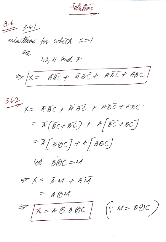
Solution:
3.4.1 AND 3.4.2
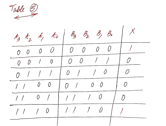
AS CAN BE CONCLUDED FROM TABLE 5....FOR FIRST AND THE LAST COMBINATION THE INPUTS ARE SAME AND THE LED GLOWS
BINARY INPUTS IN THE ORDER A3 A2 A1 A0 B3 B2 B1 B0
0000 0000

0010 0011
0111 0110
1100 0100
1101 1110
1110 1110

TABLE 5
---------------------------------------------------------------------------------------------------------------------------
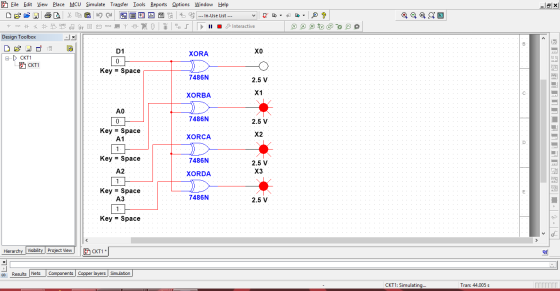
PART 3.5.1 AND 3.5.2
OUTPUTS
X3 X2 X1 X0 FOR
D1 = 0 AND
A3 A2 A1 A0 = 0000
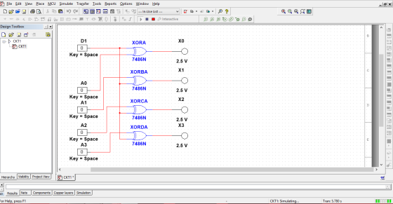
A3 A2 A1 A0 = 0010

A3 A2 A1 A0 = 0111
A3 A2 A1 A0 = 1100
A3 A2 A1 A0 = 1101
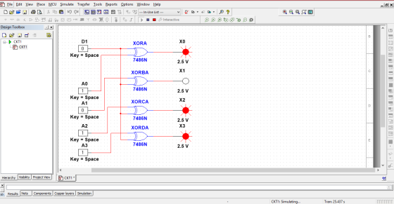
A3 A2 A1 A0 = 1110
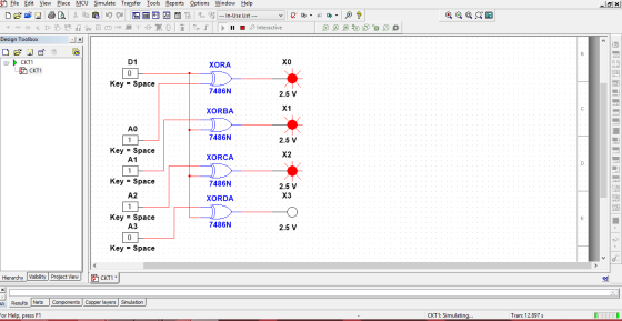
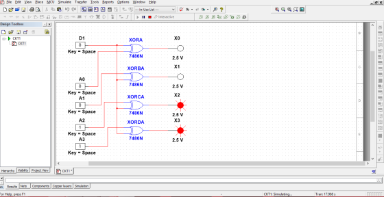
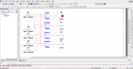
OUTPUTS
X3 X2 X1 X0 FOR
D1 = 1 AND
A3 A2 A1 A0 = 0000
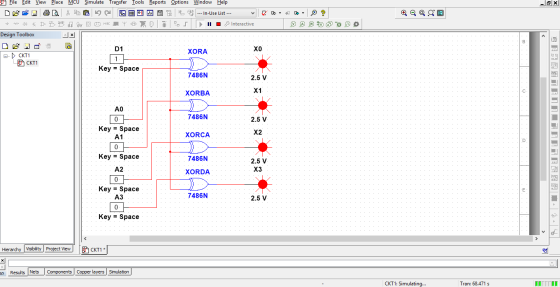
A3 A2 A1 A0 = 0010

A3 A2 A1 A0 = 0111

A3 A2 A1 A0 = 1100

A3 A2 A1 A0 = 1101

A3 A2 A1 A0 = 1110
------------------------------------------------------------------------------------------------------------------------
PART 3.6
Add Answer to:
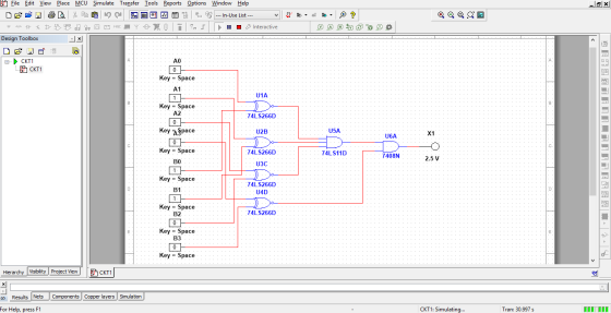
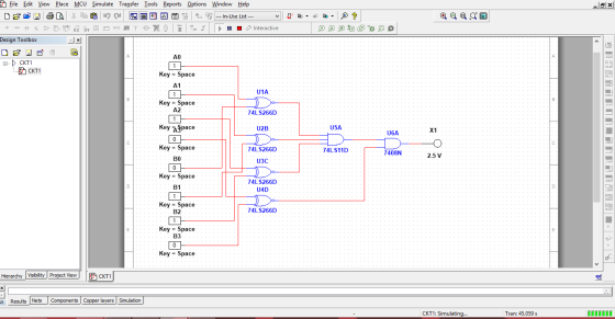
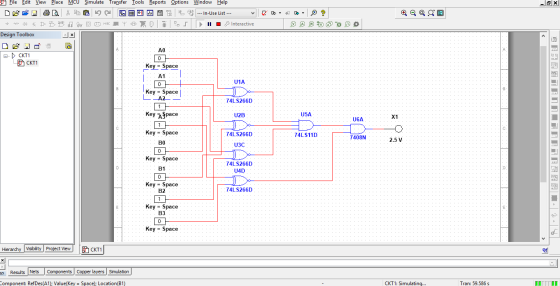
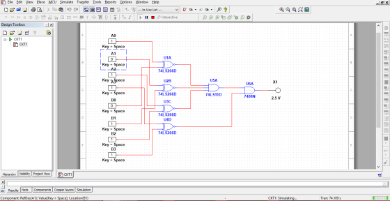
3.4.1 Build and simulate the comparator circuit shown in Figure 3, in Multisim. The inputs A3,...
3. PRELAB 1. A half adder is a circuit that has two inputs, A and B,...
 3. PRELAB 1. A half adder is a circuit that has two inputs, A and B, and two outputs, sum and carry. It adds A and B according to the rules of binary addition and outputs the sum and carry. Design a half-adder circuit using one XOR gate and one AND gate. Verify your design through truth table and with Multisim. 2. Whereas the half adder added two inputs A and B, the full adder adds three inputs together, A,...
A Y = A ® B 1 1 1 1 1 Apply the idea of the truth table above and design a 3-bit comparator using XOR or XNOR gates of...
 A Y = A ® B 1 1 1 1 1 Apply the idea of the truth table above and design a 3-bit comparator using XOR or XNOR gates of your choice. The design should be able to determine the equality between two 3-bit words. An LED should be turned ON only when every bit in "Word A" matches every corresponding bit in "Word B". Otherwise, the LED has to be OFF Hint for I/O port Definitions: Port Name Direction...
In Multisim, rewire your opamp circuit so that it matches the circuit in Figure 2 U1-....
 In Multisim, rewire your opamp circuit so that it matches the circuit in Figure 2 U1-. V4 1kn 0.707 Vrms z OPAMP 3T BASIC R1 0o Figure 2 10. Perform a transient analysis on the circuit. Plot both the input signal (node 3 in Figure 1), and the output (node 1 in Figure 1) on the same graph. Set the time start and end time of the plot to start at zero and run for approximately two cycles of the...
Truth Table Wire up the following 2-bit adder circuit shown in Figure 2. Connect the inputs...
 Truth Table
Wire up the following 2-bit adder circuit shown in Figure 2. Connect the inputs to the logic switches on the proto-burnd and the outputs to the LED indicators. Fill out a truth table for all 16 combinations of the input switches, and verify that the circuit behaves as expected Disconnect the Ao bit from the switch and connect it to the TTL function generator. Set bit A1 to 0 and Bo and B to . Measure the propagation...
Truth Table
Wire up the following 2-bit adder circuit shown in Figure 2. Connect the inputs to the logic switches on the proto-burnd and the outputs to the LED indicators. Fill out a truth table for all 16 combinations of the input switches, and verify that the circuit behaves as expected Disconnect the Ao bit from the switch and connect it to the TTL function generator. Set bit A1 to 0 and Bo and B to . Measure the propagation...
Help me please. How can I do this question. Consider the circuit shown in (Figure 1)....
 Help me please. How can I do this question.
Consider the circuit shown in (Figure 1). Suppose that ig equals 9e-5 A. Part A Use the Fourier transform to find i, (t). Suppose that io (t) = Aje-atu(t) + A2e-02* u(t) + Azeztul-t), where az > 21. Determine the va of Aj, aj, A2, a2, A3, and az. Express your answers using three significant figures separated by commas. Express A2, and A3 in amperes. Express 21, 22, and as in...
Help me please. How can I do this question.
Consider the circuit shown in (Figure 1). Suppose that ig equals 9e-5 A. Part A Use the Fourier transform to find i, (t). Suppose that io (t) = Aje-atu(t) + A2e-02* u(t) + Azeztul-t), where az > 21. Determine the va of Aj, aj, A2, a2, A3, and az. Express your answers using three significant figures separated by commas. Express A2, and A3 in amperes. Express 21, 22, and as in...
EE252 100 Points Digital Design I Two's Complement Subtraction and Add / Subtract Circuits Homework 3....
 EE252 100 Points Digital Design I Two's Complement Subtraction and Add / Subtract Circuits Homework 3. (25 Pts) The following circuit uses two 7483 (4-bit adder) ICs, labeled 7483-1 and 7483-2, respectively. Answer the questions for EACH of the following THREE CASES: Case 1: D=0010, and E = 0110 Case 2: D = 1000, and E = 0101 Case 3: D = 1000, and E = 1001 a. (6 Pts - 2 Pts per Case) What are the binary inputs...
I need help completing this in multisim 8. Load the circuit E6B-3.MS7, shown in Figure 6B.3....
 I need help completing this in multisim
8. Load the circuit E6B-3.MS7, shown in Figure 6B.3. Page 2 of 4 Module 3: Laboratory 2B: Shift Registers .5V 41958 Figure 6B.3: Pseudorandom pattem generator 9. Simulate the circuit. Record the output patterns in Table 6B.1. Pattern ABCD Pattern ABCD 10 12 13 14 15 Table 6B.1: Pattem generator output patterns 0. Experiment with different feedback imputs for the XNOR gate. What do you find?
I need help completing this in multisim
8. Load the circuit E6B-3.MS7, shown in Figure 6B.3. Page 2 of 4 Module 3: Laboratory 2B: Shift Registers .5V 41958 Figure 6B.3: Pseudorandom pattem generator 9. Simulate the circuit. Record the output patterns in Table 6B.1. Pattern ABCD Pattern ABCD 10 12 13 14 15 Table 6B.1: Pattem generator output patterns 0. Experiment with different feedback imputs for the XNOR gate. What do you find?
Q5) A combinational circuit with internal signals and signal propagation delays Shown below is a combination...
 Q5) A combinational circuit with internal signals and signal propagation delays Shown below is a combination circuit that takes 5 inputs (LO L1, L2, L3, and Comp), and generates 4 outputs (L4, L5, L6, し7) Please design the entity as well as the test bench for this combinational circuit. In your design, please set up internal signals Al, B, A2, B2, A3, B3, A4, B4, A5, B5, A6, B6, A7 and B7 Your entity design is Your test bench design...
microprocessors,,pls help.. 1. (3 Points) Draw a timing diagram similar to the 'practical' case of figure...
 microprocessors,,pls help..
1. (3 Points) Draw a timing diagram similar to the 'practical' case of figure 5, below, for the case where signal Ao makes its transition first. Note: For each timing diagram that you draw, be sure that subsequent events appear to the right of causative events, and show causality arrows. 3.1 Glitch pulses Consider the one-bit adder circuit of figure 4. This circuit is called a one-bit (binary) adder because output signal So is the sum of input...
microprocessors,,pls help..
1. (3 Points) Draw a timing diagram similar to the 'practical' case of figure 5, below, for the case where signal Ao makes its transition first. Note: For each timing diagram that you draw, be sure that subsequent events appear to the right of causative events, and show causality arrows. 3.1 Glitch pulses Consider the one-bit adder circuit of figure 4. This circuit is called a one-bit (binary) adder because output signal So is the sum of input...
Could you please read 7483 data sheet and then answer number e 7383 Data Sheet 5483A...
 Could you please read 7483 data sheet and then answer number
e
7383 Data Sheet
5483A 4-Bit Binary Full Adder with Fast Carry General Description The '83A high speed 4-bit binary full adders with internal carry lookahead accept two 4-bit binary words (Ao-A3, Bo- B3) and a Carry input (Co). They generate the binary Sum outputs (So-S3) and the Carry output (C4) from the most significant bit. They operate with either HIGH or active LOW operands (positive or negative logic)....
Could you please read 7483 data sheet and then answer number
e
7383 Data Sheet
5483A 4-Bit Binary Full Adder with Fast Carry General Description The '83A high speed 4-bit binary full adders with internal carry lookahead accept two 4-bit binary words (Ao-A3, Bo- B3) and a Carry input (Co). They generate the binary Sum outputs (So-S3) and the Carry output (C4) from the most significant bit. They operate with either HIGH or active LOW operands (positive or negative logic)....
 3. PRELAB 1. A half adder is a circuit that has two inputs, A and B, and two outputs, sum and carry. It adds A and B according to the rules of binary addition and outputs the sum and carry. Design a half-adder circuit using one XOR gate and one AND gate. Verify your design through truth table and with Multisim. 2. Whereas the half adder added two inputs A and B, the full adder adds three inputs together, A,...
 A Y = A ® B 1 1 1 1 1 Apply the idea of the truth table above and design a 3-bit comparator using XOR or XNOR gates of your choice. The design should be able to determine the equality between two 3-bit words. An LED should be turned ON only when every bit in "Word A" matches every corresponding bit in "Word B". Otherwise, the LED has to be OFF Hint for I/O port Definitions: Port Name Direction...
 In Multisim, rewire your opamp circuit so that it matches the circuit in Figure 2 U1-. V4 1kn 0.707 Vrms z OPAMP 3T BASIC R1 0o Figure 2 10. Perform a transient analysis on the circuit. Plot both the input signal (node 3 in Figure 1), and the output (node 1 in Figure 1) on the same graph. Set the time start and end time of the plot to start at zero and run for approximately two cycles of the...
 Truth Table
Wire up the following 2-bit adder circuit shown in Figure 2. Connect the inputs to the logic switches on the proto-burnd and the outputs to the LED indicators. Fill out a truth table for all 16 combinations of the input switches, and verify that the circuit behaves as expected Disconnect the Ao bit from the switch and connect it to the TTL function generator. Set bit A1 to 0 and Bo and B to . Measure the propagation...
Truth Table
Wire up the following 2-bit adder circuit shown in Figure 2. Connect the inputs to the logic switches on the proto-burnd and the outputs to the LED indicators. Fill out a truth table for all 16 combinations of the input switches, and verify that the circuit behaves as expected Disconnect the Ao bit from the switch and connect it to the TTL function generator. Set bit A1 to 0 and Bo and B to . Measure the propagation...
 Help me please. How can I do this question.
Consider the circuit shown in (Figure 1). Suppose that ig equals 9e-5 A. Part A Use the Fourier transform to find i, (t). Suppose that io (t) = Aje-atu(t) + A2e-02* u(t) + Azeztul-t), where az > 21. Determine the va of Aj, aj, A2, a2, A3, and az. Express your answers using three significant figures separated by commas. Express A2, and A3 in amperes. Express 21, 22, and as in...
Help me please. How can I do this question.
Consider the circuit shown in (Figure 1). Suppose that ig equals 9e-5 A. Part A Use the Fourier transform to find i, (t). Suppose that io (t) = Aje-atu(t) + A2e-02* u(t) + Azeztul-t), where az > 21. Determine the va of Aj, aj, A2, a2, A3, and az. Express your answers using three significant figures separated by commas. Express A2, and A3 in amperes. Express 21, 22, and as in...
 EE252 100 Points Digital Design I Two's Complement Subtraction and Add / Subtract Circuits Homework 3. (25 Pts) The following circuit uses two 7483 (4-bit adder) ICs, labeled 7483-1 and 7483-2, respectively. Answer the questions for EACH of the following THREE CASES: Case 1: D=0010, and E = 0110 Case 2: D = 1000, and E = 0101 Case 3: D = 1000, and E = 1001 a. (6 Pts - 2 Pts per Case) What are the binary inputs...
 I need help completing this in multisim
8. Load the circuit E6B-3.MS7, shown in Figure 6B.3. Page 2 of 4 Module 3: Laboratory 2B: Shift Registers .5V 41958 Figure 6B.3: Pseudorandom pattem generator 9. Simulate the circuit. Record the output patterns in Table 6B.1. Pattern ABCD Pattern ABCD 10 12 13 14 15 Table 6B.1: Pattem generator output patterns 0. Experiment with different feedback imputs for the XNOR gate. What do you find?
I need help completing this in multisim
8. Load the circuit E6B-3.MS7, shown in Figure 6B.3. Page 2 of 4 Module 3: Laboratory 2B: Shift Registers .5V 41958 Figure 6B.3: Pseudorandom pattem generator 9. Simulate the circuit. Record the output patterns in Table 6B.1. Pattern ABCD Pattern ABCD 10 12 13 14 15 Table 6B.1: Pattem generator output patterns 0. Experiment with different feedback imputs for the XNOR gate. What do you find?
 Q5) A combinational circuit with internal signals and signal propagation delays Shown below is a combination circuit that takes 5 inputs (LO L1, L2, L3, and Comp), and generates 4 outputs (L4, L5, L6, し7) Please design the entity as well as the test bench for this combinational circuit. In your design, please set up internal signals Al, B, A2, B2, A3, B3, A4, B4, A5, B5, A6, B6, A7 and B7 Your entity design is Your test bench design...
 microprocessors,,pls help..
1. (3 Points) Draw a timing diagram similar to the 'practical' case of figure 5, below, for the case where signal Ao makes its transition first. Note: For each timing diagram that you draw, be sure that subsequent events appear to the right of causative events, and show causality arrows. 3.1 Glitch pulses Consider the one-bit adder circuit of figure 4. This circuit is called a one-bit (binary) adder because output signal So is the sum of input...
microprocessors,,pls help..
1. (3 Points) Draw a timing diagram similar to the 'practical' case of figure 5, below, for the case where signal Ao makes its transition first. Note: For each timing diagram that you draw, be sure that subsequent events appear to the right of causative events, and show causality arrows. 3.1 Glitch pulses Consider the one-bit adder circuit of figure 4. This circuit is called a one-bit (binary) adder because output signal So is the sum of input...
 Could you please read 7483 data sheet and then answer number
e
7383 Data Sheet
5483A 4-Bit Binary Full Adder with Fast Carry General Description The '83A high speed 4-bit binary full adders with internal carry lookahead accept two 4-bit binary words (Ao-A3, Bo- B3) and a Carry input (Co). They generate the binary Sum outputs (So-S3) and the Carry output (C4) from the most significant bit. They operate with either HIGH or active LOW operands (positive or negative logic)....
Could you please read 7483 data sheet and then answer number
e
7383 Data Sheet
5483A 4-Bit Binary Full Adder with Fast Carry General Description The '83A high speed 4-bit binary full adders with internal carry lookahead accept two 4-bit binary words (Ao-A3, Bo- B3) and a Carry input (Co). They generate the binary Sum outputs (So-S3) and the Carry output (C4) from the most significant bit. They operate with either HIGH or active LOW operands (positive or negative logic)....
Most questions answered within 3 hours.
-
An unknown amount of a compound with a molecular mass of 284.04
g/mol is dissolved in...
asked 1 minute ago -
You are at rest at a stop sign. There is another stop sign that
is 100...
asked 2 minutes ago -
Calculate the equilibrium electrode potential for Fe3+/Fe2+
redox system, if the initial concentration of Fe2+ is...
asked 5 minutes ago -
Describe in detail with graph and diagram how bonding force,
bonding curves and bonding energy at...
asked 22 minutes ago -
Gingerbread cookies become inedible if not eaten quickly enough.
Clarence is trying to determine how many...
asked 18 minutes ago -
A
crane lifts a 200 kg block a height of 10 m in 18 seconds. What...
asked 21 minutes ago -
A 12.0-g bullet is fired horizontally into a 115-g wooden block
that is initially at rest...
asked 21 minutes ago -
Which DNA primer would have the HIGHEST melting temperature?
Question 17 options:
a)
GCATCGGC
b)
AATCGGAT...
asked 29 minutes ago -
what is the charge on the chromium ion in Cr2O3.
a -3
b -2
c 0...
asked 29 minutes ago -
which of the following may lead to speciation?
a. a group of individuals from a mainland...
asked 34 minutes ago -
Please I need today answer for This question and it is very
important and I need...
asked 53 minutes ago -
Five years from today, you plan to invest $3,700 for 7
additional years at 5.8 percent...
asked 53 minutes ago