

Homework Answers

![@ fi = Rollez)/ Ao = 30k|| 2ck?) 843-75 = 10k/1 243.75 ® +R; = 838-1] by voltage division sule Vi = hi xus tage of Rithe _238](http://img.homeworklib.com/questions/463b1130-7897-11eb-8b2a-0b378b64713f.png?x-oss-process=image/resize,w_560)
Add Answer to:
WA R3 W Consider the above circuit with indicated parameters and Rs.83.50, R1=20k0, R2=2020, RE1=428.30, RE2-5000,...
4. Consider the BJT cascade amplifier shown below Vcc 18V R1 3.3ko 15uF r Vo RL...
 4. Consider the BJT cascade amplifier shown below Vcc 18V R1 3.3ko 15uF r Vo RL B 150 Rsa 500? 56k? Vi B 150 C1 CE 2.2k? a) Find the DC collector current (approximately the same in both transistors). b) Find the input impedance, output impedance, and no-load voltage gain. c) Find the Av, Avs, and Ai d) Estimate the lower cutoff frequency e) Why does this amplifier have better high-frequency performance thana common-emitter built using the same type of...
For the circuit shown below, let Vcc 9 V R2 RE-0.11 kQ, R1 3.6 k2. and R2 -5.6 kQ. The transistor parameters are β-200, VBE(on)-OTV, VA-100 V and VT = 0.026 V. (a) Determine the quiescent value o...
 For the circuit shown below, let Vcc 9 V R2 RE-0.11 kQ, R1 3.6 k2. and R2 -5.6 kQ. The transistor parameters are β-200, VBE(on)-OTV, VA-100 V and VT = 0.026 V. (a) Determine the quiescent value of IEQ (b) Find the small-signal voltage gain Av Vo/vs (c) Determine the output resistance R, looking into output terminals Av= 0.5589 Ro-0.4688 Ω Ro-0.9118 Ω leQ- 23.76 mA Ra " 0.6538 Ω leo 39.52 mA A, 0.9938
For the circuit shown below,...
For the circuit shown below, let Vcc 9 V R2 RE-0.11 kQ, R1 3.6 k2. and R2 -5.6 kQ. The transistor parameters are β-200, VBE(on)-OTV, VA-100 V and VT = 0.026 V. (a) Determine the quiescent value of IEQ (b) Find the small-signal voltage gain Av Vo/vs (c) Determine the output resistance R, looking into output terminals Av= 0.5589 Ro-0.4688 Ω Ro-0.9118 Ω leQ- 23.76 mA Ra " 0.6538 Ω leo 39.52 mA A, 0.9938
For the circuit shown below,...
Avec Úvo SRE L V II. (5pt) Consider the above-right common-collector or emitter-follower BJT amplifier circuit....
 Avec Úvo SRE L V II. (5pt) Consider the above-right common-collector or emitter-follower BJT amplifier circuit. Given: ß= 100, RE = 10 k1, Vcc = 20 V, RB = 5 k1, R1 = 10 kl, and Ry = 2 k1. (a) (1pt) Find the Q-point, i.e. Ibo, Ico, and VCEO; (b) (1pt) draw the small-signal equivalent circuit assuming that the capacitors (C, and Cy) are short circuits for the small signal; (c) (1pt) solve for the voltage gain, Av; (d)...
1. Consider the Common-Emitter BJT amplifier circuit, shown below. VD VOD BJT Parameters: B=99 A/A i=0...
 1. Consider the Common-Emitter BJT amplifier circuit, shown below. VD VOD BJT Parameters: B=99 A/A i=0 RE Co Circuit Parameters: Ca Cc2 = 0 F Car = OF R = 2022 R = 2002 R1 = 25.8 k22 Ry2 = 51.6 ks V = 15 V VEE=0 V Сct Active Mode: Va >0.2 V Vwx=0.7V Ic=B1, Ic=al, 1 R2 3 SRCA a) Find the open-circuit voltage gain, Ave, of this amplifier circuit. Verify your assumptions. b) Compute the input resistance,...
Design a BJT amplifier based on the specifications provided in the table below. Your design shoul...
 THE STEPS TO DO SO:
Design a BJT amplifier based on the specifications provided in the table below. Your design should be insensitive to β variations, and both the input and the output should be AC coupled as in Fig. 1. Supply Voltage, Vcc Load Resistance, RL Transistor's Current Gain, β Relative Variation of lc for VBE-0.7 ± 0.1 V 0-to-Peak Output Swing, Vo Voltage Gain, A Input Resistance, R THD for 5kHz IV (0-to-peak) Sine Wave Output Voltage, V。S5%...
THE STEPS TO DO SO:
Design a BJT amplifier based on the specifications provided in the table below. Your design should be insensitive to β variations, and both the input and the output should be AC coupled as in Fig. 1. Supply Voltage, Vcc Load Resistance, RL Transistor's Current Gain, β Relative Variation of lc for VBE-0.7 ± 0.1 V 0-to-Peak Output Swing, Vo Voltage Gain, A Input Resistance, R THD for 5kHz IV (0-to-peak) Sine Wave Output Voltage, V。S5%...
Question 4 (25 Marks) (5) 1. Derive the Dynamic Emitter Resistance, re that is used in...
 Question 4 (25 Marks) (5) 1. Derive the Dynamic Emitter Resistance, re that is used in the re-model small-signal analysis of BJT. 2. The circuit in Figure 7 shows the multistage cascade of two single transistors with B=100. Given the value of Vpp=12 V, R1=120 kN, R2=40 kN, R3=100 ks, Ra=30 kn, RE1=3.9 kN, Rez=4.5 kN, Rc1=6.5 kN, Rc2=8 ks, (2) (4) (a) Identify the transistor configuration for all stages. (b) Determine the d.c collector current (Ici and I cz)...
Vcc= 15 V Rc 2 kO R1 10 kO Vo C1 R2=5 kQ Vs RE= 2...
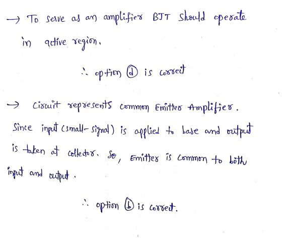
 Vcc= 15 V Rc 2 kO R1 10 kO Vo C1 R2=5 kQ Vs RE= 2 kQ Figure 1.1 [Rajah 1.1) SECTION A Bakagian A Question 1 Soalan 1 State THREE (3) operating regions in Bipolar Junction Transistor (BJT) and (a) briefly explain. [Nyatakan TIGA (3) kawasan operasi untuk transistor simpang dwikutub (BJT) dan jelaskan.] (3 Marks/Markah) (b) Based on the Figure 1.1, given B 100 and VBE (ON) 0.7 V. [Berdasarkan Rajah 1.1, diberi B 100 dan Vas (ON...
Vcc= 15 V Rc 2 kO R1 10 kO Vo C1 R2=5 kQ Vs RE= 2...
 Vcc= 15 V Rc 2 kO R1 10 kO Vo C1 R2=5 kQ Vs RE= 2 kQ Figure 1.1 [Rajah 1.1) SECTION A Bakagian A Question 1 Soalan 1 State THREE (3) operating regions in Bipolar Junction Transistor (BJT) and (a) briefly explain. [Nyatakan TIGA (3) kawasan operasi untuk transistor simpang dwikutub (BJT) dan jelaskan.] (3 Marks/Markah) (b) Based on the Figure 1.1, given B 100 and VBE (ON) 0.7 V. [Berdasarkan Rajah 1.1, diberi B 100 dan Vas (ON...
can you do 4.83 Ar- Q Sea 100 V, what does the gain become? age at...
 can
you do 4.83
Ar- Q Sea 100 V, what does the gain become? age at the collector. (b) Replacing the transistor by its T model, da the small-signal equivalent circuit of the a plifier. Analyze the resulting circuit to dete mine the voltage gain t/ 04.81 Consider the CE amplifier circuit of Fig. 4.43(a). It is required to design the circuit (i.e., find values for I and Rc) to meet the following specifications: (a) R,5kn (b) the voltage gain...
can
you do 4.83
Ar- Q Sea 100 V, what does the gain become? age at the collector. (b) Replacing the transistor by its T model, da the small-signal equivalent circuit of the a plifier. Analyze the resulting circuit to dete mine the voltage gain t/ 04.81 Consider the CE amplifier circuit of Fig. 4.43(a). It is required to design the circuit (i.e., find values for I and Rc) to meet the following specifications: (a) R,5kn (b) the voltage gain...
Problem 2: In the circuit on Figure P2, BJT NPN Q1 and Q2 emulate a Darlington...
 Problem 2: In the circuit on Figure P2, BJT NPN Q1 and Q2 emulate a Darlington Pair (DP). It should be noted that Q1 and Q2 are such that their current gains are B1 B2 = B = 99. Moreover, capacitors C1 and C2 can be assumed to be very large. Note: The DC analysis of the DP circuit below can be done in a similar fashion as what you do when only dealing with one transistor. Express the current...
 4. Consider the BJT cascade amplifier shown below Vcc 18V R1 3.3ko 15uF r Vo RL B 150 Rsa 500? 56k? Vi B 150 C1 CE 2.2k? a) Find the DC collector current (approximately the same in both transistors). b) Find the input impedance, output impedance, and no-load voltage gain. c) Find the Av, Avs, and Ai d) Estimate the lower cutoff frequency e) Why does this amplifier have better high-frequency performance thana common-emitter built using the same type of...
 For the circuit shown below, let Vcc 9 V R2 RE-0.11 kQ, R1 3.6 k2. and R2 -5.6 kQ. The transistor parameters are β-200, VBE(on)-OTV, VA-100 V and VT = 0.026 V. (a) Determine the quiescent value of IEQ (b) Find the small-signal voltage gain Av Vo/vs (c) Determine the output resistance R, looking into output terminals Av= 0.5589 Ro-0.4688 Ω Ro-0.9118 Ω leQ- 23.76 mA Ra " 0.6538 Ω leo 39.52 mA A, 0.9938
For the circuit shown below,...
For the circuit shown below, let Vcc 9 V R2 RE-0.11 kQ, R1 3.6 k2. and R2 -5.6 kQ. The transistor parameters are β-200, VBE(on)-OTV, VA-100 V and VT = 0.026 V. (a) Determine the quiescent value of IEQ (b) Find the small-signal voltage gain Av Vo/vs (c) Determine the output resistance R, looking into output terminals Av= 0.5589 Ro-0.4688 Ω Ro-0.9118 Ω leQ- 23.76 mA Ra " 0.6538 Ω leo 39.52 mA A, 0.9938
For the circuit shown below,...
 Avec Úvo SRE L V II. (5pt) Consider the above-right common-collector or emitter-follower BJT amplifier circuit. Given: ß= 100, RE = 10 k1, Vcc = 20 V, RB = 5 k1, R1 = 10 kl, and Ry = 2 k1. (a) (1pt) Find the Q-point, i.e. Ibo, Ico, and VCEO; (b) (1pt) draw the small-signal equivalent circuit assuming that the capacitors (C, and Cy) are short circuits for the small signal; (c) (1pt) solve for the voltage gain, Av; (d)...
 1. Consider the Common-Emitter BJT amplifier circuit, shown below. VD VOD BJT Parameters: B=99 A/A i=0 RE Co Circuit Parameters: Ca Cc2 = 0 F Car = OF R = 2022 R = 2002 R1 = 25.8 k22 Ry2 = 51.6 ks V = 15 V VEE=0 V Сct Active Mode: Va >0.2 V Vwx=0.7V Ic=B1, Ic=al, 1 R2 3 SRCA a) Find the open-circuit voltage gain, Ave, of this amplifier circuit. Verify your assumptions. b) Compute the input resistance,...
 THE STEPS TO DO SO:
Design a BJT amplifier based on the specifications provided in the table below. Your design should be insensitive to β variations, and both the input and the output should be AC coupled as in Fig. 1. Supply Voltage, Vcc Load Resistance, RL Transistor's Current Gain, β Relative Variation of lc for VBE-0.7 ± 0.1 V 0-to-Peak Output Swing, Vo Voltage Gain, A Input Resistance, R THD for 5kHz IV (0-to-peak) Sine Wave Output Voltage, V。S5%...
THE STEPS TO DO SO:
Design a BJT amplifier based on the specifications provided in the table below. Your design should be insensitive to β variations, and both the input and the output should be AC coupled as in Fig. 1. Supply Voltage, Vcc Load Resistance, RL Transistor's Current Gain, β Relative Variation of lc for VBE-0.7 ± 0.1 V 0-to-Peak Output Swing, Vo Voltage Gain, A Input Resistance, R THD for 5kHz IV (0-to-peak) Sine Wave Output Voltage, V。S5%...
 Question 4 (25 Marks) (5) 1. Derive the Dynamic Emitter Resistance, re that is used in the re-model small-signal analysis of BJT. 2. The circuit in Figure 7 shows the multistage cascade of two single transistors with B=100. Given the value of Vpp=12 V, R1=120 kN, R2=40 kN, R3=100 ks, Ra=30 kn, RE1=3.9 kN, Rez=4.5 kN, Rc1=6.5 kN, Rc2=8 ks, (2) (4) (a) Identify the transistor configuration for all stages. (b) Determine the d.c collector current (Ici and I cz)...
 Vcc= 15 V Rc 2 kO R1 10 kO Vo C1 R2=5 kQ Vs RE= 2 kQ Figure 1.1 [Rajah 1.1) SECTION A Bakagian A Question 1 Soalan 1 State THREE (3) operating regions in Bipolar Junction Transistor (BJT) and (a) briefly explain. [Nyatakan TIGA (3) kawasan operasi untuk transistor simpang dwikutub (BJT) dan jelaskan.] (3 Marks/Markah) (b) Based on the Figure 1.1, given B 100 and VBE (ON) 0.7 V. [Berdasarkan Rajah 1.1, diberi B 100 dan Vas (ON...
 Vcc= 15 V Rc 2 kO R1 10 kO Vo C1 R2=5 kQ Vs RE= 2 kQ Figure 1.1 [Rajah 1.1) SECTION A Bakagian A Question 1 Soalan 1 State THREE (3) operating regions in Bipolar Junction Transistor (BJT) and (a) briefly explain. [Nyatakan TIGA (3) kawasan operasi untuk transistor simpang dwikutub (BJT) dan jelaskan.] (3 Marks/Markah) (b) Based on the Figure 1.1, given B 100 and VBE (ON) 0.7 V. [Berdasarkan Rajah 1.1, diberi B 100 dan Vas (ON...
 can
you do 4.83
Ar- Q Sea 100 V, what does the gain become? age at the collector. (b) Replacing the transistor by its T model, da the small-signal equivalent circuit of the a plifier. Analyze the resulting circuit to dete mine the voltage gain t/ 04.81 Consider the CE amplifier circuit of Fig. 4.43(a). It is required to design the circuit (i.e., find values for I and Rc) to meet the following specifications: (a) R,5kn (b) the voltage gain...
can
you do 4.83
Ar- Q Sea 100 V, what does the gain become? age at the collector. (b) Replacing the transistor by its T model, da the small-signal equivalent circuit of the a plifier. Analyze the resulting circuit to dete mine the voltage gain t/ 04.81 Consider the CE amplifier circuit of Fig. 4.43(a). It is required to design the circuit (i.e., find values for I and Rc) to meet the following specifications: (a) R,5kn (b) the voltage gain...
 Problem 2: In the circuit on Figure P2, BJT NPN Q1 and Q2 emulate a Darlington Pair (DP). It should be noted that Q1 and Q2 are such that their current gains are B1 B2 = B = 99. Moreover, capacitors C1 and C2 can be assumed to be very large. Note: The DC analysis of the DP circuit below can be done in a similar fashion as what you do when only dealing with one transistor. Express the current...
Most questions answered within 3 hours.
-
You are attempting to calculate a firm’s free cash flow to
equity. You know the following...
asked 50 minutes ago -
the following reaction occurs in a balloon containing
N2O2 gas
N2O4(g)=2NO2(g)
will the volume of the...
asked 1 hour ago -
answer the questions throughout this program
public class Day implements Comparable {
Private Boolean atWork;...
asked 1 hour ago -
This is C++ code for parking fee management program
#include <iostream>
#include <iomanip>
using namespace std;...
asked 1 hour ago -
The free energy change for the following reaction at 25 °C, when
[Sn2+] = 1.17 M...
asked 3 hours ago -
An MNE is this kind of industry when competition in one country
is essentially independent of...
asked 5 hours ago -
. For this set of questions, determine what
proportion of a normal distribution is located betweeneach...
asked 5 hours ago -
A college student is employed as a door-to-door newspaper
salesman. Historical data suggests that the student...
asked 6 hours ago -
MATLAB HW 11 problem using Switch Case and Input commands
Write a script file that calculates...
asked 6 hours ago -
Considering gravitational time dilation, calculate the time that
passes in Earth’s surface while 1 hour passes...
asked 6 hours ago -
Minitab Problem: Take the Lake Hume June rainfall data and find
use the processes outlined in...
asked 7 hours ago -
X Company is trying to decide whether to continue using old
equipment to make Product A...
asked 7 hours ago