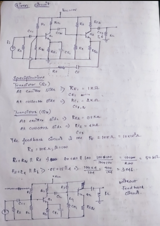
For the given circuit below (transistor parameters are Beta = 100, Rs = 10 kOhm).
a) From the given bias conditions, calculate the necessary parameters for equivalent circuits.
b) Identify:
1) the feedback circuit,
2) find the feedback coefficient,
3) input loading resistor Rif,
4) output loading resistor Rof.
c) Draw an equivalent circuit without feedback and simulate.
d) Draw an equivalent circuit with loading resistors and without feedback.
e) Draw the equivalent circuit with feedback.
d) Explain that your circuits verify the feedback
concept.
Homework Answers
Add Answer to:
For the given circuit below (transistor parameters are Beta =
100, Rs = 10 kOhm).
a)...
Figure Qlc) below shows a transistor amplifier circuit in which the quiescent DC collector current is...
 Figure Qlc) below shows a transistor amplifier circuit in which the quiescent DC collector current is ImA (the bias resistors are omitted). Assuming that rce and RE are large enough to be neglected, draw the equivalent circuit and calculate the voltage gain, v/r. State an application for this amplifier. The collector resistor, Re Rc 0 RE 0V Figure Q1c)
For all BJTs, assume: IVBE,on1-0.7V, β 100, and|VCE,sat-0.1V (use Vr 25mV) For all MOSFETs, assume: I'm|-1V...
 For all BJTs, assume: IVBE,on1-0.7V, β 100, and|VCE,sat-0.1V (use Vr 25mV) For all MOSFETs, assume: I'm|-1V and μ COX-20 V2. Q3: Consider the circuit shown to the right where W- 100. Resistor values are: RG 1M, RD 10kn, Rs 500, R 20k0, and Rs 100k. The capacitors should be assumed short- circuits at the operating frequency of the circuit and Vo -Vss = +3V. a) Calculate the bias point parameters (lo and Vos) for the Rai Ca Rsi transistor and...
Question 1: 7.33 +15V 1O MO R-200k 16n 7k MO 7.33 Figure P7.33 shows a discrete-circuit...
 Question 1: 7.33 +15V 1O MO R-200k 16n 7k MO 7.33 Figure P7.33 shows a discrete-circuit amplifier. The input signal is coupled to the gate through a very large capacitor (shown as infinite). The transistor source is connected to ground at signal frequencies via a very large capacitor (shown as infinite). The output voltage signal that develops at the drain is coupled to a load resistance via a very large capacitor (shown as infinite). All capacitors behave as short circuits...
In the circuit of given below, Vsig is a small sine wave signal with zero average. The transistor...
 In the circuit of given below, Vsig is a small sine wave signal with zero average. The transistor B is 100. a) Find the value of RE to establish a dc emitter current of about 0.5 mA. b) Find Rc to establish a dc collector voltage of about +5 V c) For RL10 kS2 and the transistor ro 200 k2, draw the small-signal equivalent circuit 5. of the amplifier and determine its overall voltage gain +15 V Re O Vo...
Given the circuit below with the following parameters: - M1: Vt,n = 0.48 V, Un Cox...
 Given the circuit below with the following parameters: - M1: Vt,n = 0.48 V, Un Cox = 90 UA/V2, W/L = 10 um/4 um, VdD+Vad 1 = 0.01 [1/V] - Supply voltage: Vpp = 3.3 V, vad = 10 mV > R a. Find the value of resistor R so that the bias current is 10uA. (Hint: Channel length modulation should be considered.) Ipi M1 Use the resistor value in (a) for the following calculations: b. What configuration (connection) M1...
#4 The accompanying circuit shows a 4-resistor biased JFET transistor Determine the values of Rp and Rs so that the Q-point is equal to, VDsq 10 V and IDg 5 mA . For the JFET take IDss = 10 mA...
 #4
The accompanying circuit shows a 4-resistor biased JFET transistor Determine the values of Rp and Rs so that the Q-point is equal to, VDsq 10 V and IDg 5 mA . For the JFET take IDss = 10 mA, VP =-5 V and λ 0 . The circuit parameters are, R1-740 k, R2-22 1.85 ka, Rs-85 ㏀ and RL-3.5 ㏀. Take the power supply VDD 24 V 2- Vo R1 Vi R2 Signal generator 4-In reference to the circuit...
#4
The accompanying circuit shows a 4-resistor biased JFET transistor Determine the values of Rp and Rs so that the Q-point is equal to, VDsq 10 V and IDg 5 mA . For the JFET take IDss = 10 mA, VP =-5 V and λ 0 . The circuit parameters are, R1-740 k, R2-22 1.85 ka, Rs-85 ㏀ and RL-3.5 ㏀. Take the power supply VDD 24 V 2- Vo R1 Vi R2 Signal generator 4-In reference to the circuit...
The 1 mA. V, ls -VE -15 15 V, in the following differential amplifier circuit, Vcc parameters are given as β, 100, VBE# 0.7 V, pr-25 mV, K.-100 V. transistor Rc-10 kΩ For: RE-150 Ω Rc Rc REE-200...
 The 1 mA. V, ls -VE -15 15 V, in the following differential amplifier circuit, Vcc parameters are given as β, 100, VBE# 0.7 V, pr-25 mV, K.-100 V. transistor Rc-10 kΩ For: RE-150 Ω Rc Rc REE-200 kΩ a) What is the input differential resistance, Rid b) What is the overall voltage gain vV? You c) What is input common mode resistance, d) What is the worst case common mode gain that appear across the two input terminals? (4...
Laboratory 2: Transistor circuit characteristics A. Objectives: 1. To study the basic characteris...
 Laboratory 2: Transistor circuit characteristics A. Objectives: 1. To study the basic characteristics of a transistor circuit. 2. To study the bias circuit of a transistor circuit. B. Apparatus: 1. DC Power supply 2. Experimental boards and corresponding components 3. Electronic calculator (prepared by students) 4. Digital camera (prepared by students for photo taking of the experimental results) 5. Laptop computer with the software PicoScope 6 and Microsoft Word installed. 6. PicoScope PC Oscilloscope and its accessories. 7. Digital multi-meter....
In the amplifier circuit below, the transistor has the following properties:Vt =1.5V,k’n=100 microA/V2,W=2 micro m ,L=0.2...
 In the amplifier circuit below, the transistor has the following
properties:Vt =1.5V,k’n=100 microA/V2,W=2 micro m ,L=0.2 micro m,
lambda = 0V^-1
a. Find the dc values VG, VD, and VS.
b. Verify (prove) that the circuit is in the proper region of
operation for an amplifier
c. Find the transconductance value, gm
d. Draw the equivalent small-signal circuit model, replacing the
NMOS with its pi-model
e. Draw the equivalent small-signal circuit model, replacing the
NMOS with its T-model
f. Calculate...
In the amplifier circuit below, the transistor has the following
properties:Vt =1.5V,k’n=100 microA/V2,W=2 micro m ,L=0.2 micro m,
lambda = 0V^-1
a. Find the dc values VG, VD, and VS.
b. Verify (prove) that the circuit is in the proper region of
operation for an amplifier
c. Find the transconductance value, gm
d. Draw the equivalent small-signal circuit model, replacing the
NMOS with its pi-model
e. Draw the equivalent small-signal circuit model, replacing the
NMOS with its T-model
f. Calculate...
12 = 5x 10-16 (A), 2. Consider the BJT circuit below, where Isi = 2 x...
 12 = 5x 10-16 (A), 2. Consider the BJT circuit below, where Isi = 2 x 10"""[A), B1 = 100, 1:2 = 5 x 10 B = 50, V1 = 26 [mV], VBB = 2 [V], Vcc=5 [V], R1 = 1 [kS2], and VA=0. (a) We want to operate Q2 (pnp BJT) in "soft saturation region with Base-Collect junction being forward biased by 200 [mV]. Find input supply voltage (large signal), Vsupp, and output voltage (large signal), Vout, for the...
 Figure Qlc) below shows a transistor amplifier circuit in which the quiescent DC collector current is ImA (the bias resistors are omitted). Assuming that rce and RE are large enough to be neglected, draw the equivalent circuit and calculate the voltage gain, v/r. State an application for this amplifier. The collector resistor, Re Rc 0 RE 0V Figure Q1c)
 For all BJTs, assume: IVBE,on1-0.7V, β 100, and|VCE,sat-0.1V (use Vr 25mV) For all MOSFETs, assume: I'm|-1V and μ COX-20 V2. Q3: Consider the circuit shown to the right where W- 100. Resistor values are: RG 1M, RD 10kn, Rs 500, R 20k0, and Rs 100k. The capacitors should be assumed short- circuits at the operating frequency of the circuit and Vo -Vss = +3V. a) Calculate the bias point parameters (lo and Vos) for the Rai Ca Rsi transistor and...
 Question 1: 7.33 +15V 1O MO R-200k 16n 7k MO 7.33 Figure P7.33 shows a discrete-circuit amplifier. The input signal is coupled to the gate through a very large capacitor (shown as infinite). The transistor source is connected to ground at signal frequencies via a very large capacitor (shown as infinite). The output voltage signal that develops at the drain is coupled to a load resistance via a very large capacitor (shown as infinite). All capacitors behave as short circuits...
 In the circuit of given below, Vsig is a small sine wave signal with zero average. The transistor B is 100. a) Find the value of RE to establish a dc emitter current of about 0.5 mA. b) Find Rc to establish a dc collector voltage of about +5 V c) For RL10 kS2 and the transistor ro 200 k2, draw the small-signal equivalent circuit 5. of the amplifier and determine its overall voltage gain +15 V Re O Vo...
 Given the circuit below with the following parameters: - M1: Vt,n = 0.48 V, Un Cox = 90 UA/V2, W/L = 10 um/4 um, VdD+Vad 1 = 0.01 [1/V] - Supply voltage: Vpp = 3.3 V, vad = 10 mV > R a. Find the value of resistor R so that the bias current is 10uA. (Hint: Channel length modulation should be considered.) Ipi M1 Use the resistor value in (a) for the following calculations: b. What configuration (connection) M1...
 #4
The accompanying circuit shows a 4-resistor biased JFET transistor Determine the values of Rp and Rs so that the Q-point is equal to, VDsq 10 V and IDg 5 mA . For the JFET take IDss = 10 mA, VP =-5 V and λ 0 . The circuit parameters are, R1-740 k, R2-22 1.85 ka, Rs-85 ㏀ and RL-3.5 ㏀. Take the power supply VDD 24 V 2- Vo R1 Vi R2 Signal generator 4-In reference to the circuit...
#4
The accompanying circuit shows a 4-resistor biased JFET transistor Determine the values of Rp and Rs so that the Q-point is equal to, VDsq 10 V and IDg 5 mA . For the JFET take IDss = 10 mA, VP =-5 V and λ 0 . The circuit parameters are, R1-740 k, R2-22 1.85 ka, Rs-85 ㏀ and RL-3.5 ㏀. Take the power supply VDD 24 V 2- Vo R1 Vi R2 Signal generator 4-In reference to the circuit...
 The 1 mA. V, ls -VE -15 15 V, in the following differential amplifier circuit, Vcc parameters are given as β, 100, VBE# 0.7 V, pr-25 mV, K.-100 V. transistor Rc-10 kΩ For: RE-150 Ω Rc Rc REE-200 kΩ a) What is the input differential resistance, Rid b) What is the overall voltage gain vV? You c) What is input common mode resistance, d) What is the worst case common mode gain that appear across the two input terminals? (4...
 Laboratory 2: Transistor circuit characteristics A. Objectives: 1. To study the basic characteristics of a transistor circuit. 2. To study the bias circuit of a transistor circuit. B. Apparatus: 1. DC Power supply 2. Experimental boards and corresponding components 3. Electronic calculator (prepared by students) 4. Digital camera (prepared by students for photo taking of the experimental results) 5. Laptop computer with the software PicoScope 6 and Microsoft Word installed. 6. PicoScope PC Oscilloscope and its accessories. 7. Digital multi-meter....
 In the amplifier circuit below, the transistor has the following
properties:Vt =1.5V,k’n=100 microA/V2,W=2 micro m ,L=0.2 micro m,
lambda = 0V^-1
a. Find the dc values VG, VD, and VS.
b. Verify (prove) that the circuit is in the proper region of
operation for an amplifier
c. Find the transconductance value, gm
d. Draw the equivalent small-signal circuit model, replacing the
NMOS with its pi-model
e. Draw the equivalent small-signal circuit model, replacing the
NMOS with its T-model
f. Calculate...
In the amplifier circuit below, the transistor has the following
properties:Vt =1.5V,k’n=100 microA/V2,W=2 micro m ,L=0.2 micro m,
lambda = 0V^-1
a. Find the dc values VG, VD, and VS.
b. Verify (prove) that the circuit is in the proper region of
operation for an amplifier
c. Find the transconductance value, gm
d. Draw the equivalent small-signal circuit model, replacing the
NMOS with its pi-model
e. Draw the equivalent small-signal circuit model, replacing the
NMOS with its T-model
f. Calculate...
 12 = 5x 10-16 (A), 2. Consider the BJT circuit below, where Isi = 2 x 10"""[A), B1 = 100, 1:2 = 5 x 10 B = 50, V1 = 26 [mV], VBB = 2 [V], Vcc=5 [V], R1 = 1 [kS2], and VA=0. (a) We want to operate Q2 (pnp BJT) in "soft saturation region with Base-Collect junction being forward biased by 200 [mV]. Find input supply voltage (large signal), Vsupp, and output voltage (large signal), Vout, for the...
Most questions answered within 3 hours.
-
4. Determine the theoretical yield of P2O5, when 3.07 g of P
reacts with 6.09 g...
asked 1 hour ago -
Explain the PEST analysis and how a marketer would use this when
putting together a marketing...
asked 1 hour ago -
S sells property with a $500 basis to B for $450, and B later
sells the...
asked 2 hours ago -
True/False Questions
1.
In interpreting an agreement, courts generally apply a
subjective standard.
2.
If, after...
asked 1 hour ago -
On January 1, 20X7, Green Corp. paid $1,020,000 to acquire Wax
Co. Wax maintained separate incorporation....
asked 2 hours ago -
C++
Write a class Fraction that defines adding, subtracting,
multiplying, and dividing fractions by overloading standard...
asked 3 hours ago -
This java code won't run and I can't figure out the problem with
it. Please help...
asked 4 hours ago -
Trace the following recursive methods:
a) isPal with the string “abccda”
b) isAnBn with the string...
asked 5 hours ago -
1. Which of the following is false about photosynthesis?
A. ATP is the molecule used to...
asked 6 hours ago -
A simple random sample of size n=64 is obtained from a
population with a mean of...
asked 7 hours ago -
(2 dimensions, 1 object, 2 accelerations)
1) A projectile is thrown with a wind. The wind...
asked 8 hours ago -
Brian makes $34,100 per year. How much can Brian expect to
contribute to FICA taxes in...
asked 9 hours ago