
Homework Answers


![PA SUB-VA - I (P242 ] Les LCHBW NA B (poletana) (2) II - VA VB TVAE VATIR27 R... Iver IR 2 FUB : up-va).- er Re] Europos (UB-](http://img.homeworklib.com/questions/6b367360-ac32-11eb-9d65-43a68db4b5b5.png?x-oss-process=image/resize,w_560)


Add Answer to:
1. Derive the gain expression for the following instrument amplifier shown in Figure 1. 2. Derive...
Consider the CB amplifier in figure 1 and derive an expression for its bias current IC....
 Consider the CB amplifier in figure 1 and derive an expression
for its bias current IC. Select a value for IC that guarantees a
peak-peak output swing of at least 3 V and find the corresponding
resistor values R1, R2, and RE.
RS lin ci IC 8 수 ANN + 1 오 vs © 10k Vin REŠ PT SR2 - HAI 2 | Figure 1: Common-base amplifier with finite source resistance and fixed resistive load.
Consider the CB amplifier in figure 1 and derive an expression
for its bias current IC. Select a value for IC that guarantees a
peak-peak output swing of at least 3 V and find the corresponding
resistor values R1, R2, and RE.
RS lin ci IC 8 수 ANN + 1 오 vs © 10k Vin REŠ PT SR2 - HAI 2 | Figure 1: Common-base amplifier with finite source resistance and fixed resistive load.
b) Draw an appropriate equivalent circuit for the amplifier shown in Figure Q4b, and hence derive...
 b) Draw an appropriate equivalent circuit for the amplifier shown in Figure Q4b, and hence derive the following expression for the input impedance + Ir Figure Q4b)
Find the differential half-circuit for the differential amplifier shown in Figurre and use it to derive an expression f...
 Find the differential half-circuit for the differential
amplifier shown in Figurre and use it to derive an expression for
the differential gain Ad= vod/vid in terms of gm,
RD, and RS. What is the gain with RS =0?
What is the value of RS (in terms of 1/gm) that
reduces the gain to half this value?
Find the differential half-circuit for the differential
amplifier shown in Figurre and use it to derive an expression for
the differential gain Ad= vod/vid in terms of gm,
RD, and RS. What is the gain with RS =0?
What is the value of RS (in terms of 1/gm) that
reduces the gain to half this value?
Problem 1: Derive the expression for G Eo/Ei for common amplifier circuits using op-amps (figure ...
 Problem 1: Derive the expression for G Eo/Ei for common amplifier circuits using op-amps (figure 6.20 of F&B 5th ed.; figure 6.19 of F&B 6th ed.) a. Non-inverting amplifier (see class notes) b. Inverting amplifier (see class notes) c. Differential amplifier d. Voltage follower Problem 2: A non-inverting amplifier is built using a 1-k2 precision resistors R1 and R2 (see part b from previous problem), which have a tolerance of ±1%. Determine the circuit's gain and the tolerance in the...
Problem Consider a voltage amplifier having a frequency response of the low-pass STC 1ype with a de gain of 60 dB a...
 Problem Consider a voltage amplifier having a frequency response of the low-pass STC 1ype with a de gain of 60 dB and a 3-dB frequency of 1000 Hz Find the gain in dB at f- 10 Hz, 10kHz, 100 kHz, and 1 MHz Problem For the circuit shown below first, evalusteand the coresponding comer froquency. Second evalmt and the corresponding comer froquency. At the end caloulate overall transfer function T(w)= and reurite it in the standard fom ( and draw...
For the differential amplifier shown in Figure (2),
 For the differential amplifier shown in Figure (2),assume \(\mathrm{VCC}=12 \mathrm{~V}, \mathrm{VEE}=-12 \mathrm{~V}, \mathrm{Rc}=2 \mathrm{k} \Omega\), and \(\beta=100\) for all transistors.For the current source circuit (Transistor \(\left.Q_{3}\right): R_{1}=4 k \Omega, R_{2}=4 k \Omega, R_{3}=3 \mathrm{k} \Omega\), and \(r_{0}=100 \mathrm{k} \Omega\).a) In differential amplifier circuits, what do "well-matched transistors" mean?b) Why it is important to use well-matched transistors in differential amplifier circuits?c) What are the operating \(Q\) point values \(\left(I_{c Q}\right.\) and \(\left.V_{C Q}\right)\) for the transistors \(Q_{1}\) and \(Q_{2}\) ?d) Draw...
For the differential amplifier shown in Figure 6: Assume well-matched transistors and = 100 for all transistors: a) Wh...
 For the differential amplifier shown in Figure 6: Assume
well-matched transistors and = 100 for all transistors:
a) Why it is important to use well-matched transistors in
differential amplifier circuits? What is the potential influence of
mismatched transistors on the performance of the differential
amplifier?
b) Determine the resistor values (R1, R2 and R3) such that the
emitter coupled current IE = 0.5 mA and VC1 = 3 V.
c) Draw the ac equivalent circuit for the single ended...
For the differential amplifier shown in Figure 6: Assume
well-matched transistors and = 100 for all transistors:
a) Why it is important to use well-matched transistors in
differential amplifier circuits? What is the potential influence of
mismatched transistors on the performance of the differential
amplifier?
b) Determine the resistor values (R1, R2 and R3) such that the
emitter coupled current IE = 0.5 mA and VC1 = 3 V.
c) Draw the ac equivalent circuit for the single ended...
Problem 2 Consider the feedback amplifier circuit on Figure P2. The DC current gain of transistor Q3 is -100 1. What type of feedback (or what feedback topology) do we have on the circuit in Figure P...
 Problem 2 Consider the feedback amplifier circuit on Figure P2. The DC current gain of transistor Q3 is -100 1. What type of feedback (or what feedback topology) do we have on the circuit in Figure P2? 2. Draw the A-circuit. Express and compute the open-loop voltage gain A at mid-band frequency 3, Draw the γ-circuit. Express and compute the feedback factor γ 4. Express and compute the overall gain of the feedback amplifier Ap Express and compute the input...
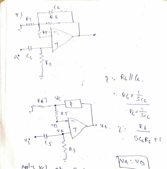
8. Derive an expression for the voltage gain, vo/vi,of the circuit in the following circuit. 1...
 8. Derive an expression for the voltage gain, vo/vi,of the circuit in the following circuit. 1 +
A common source amplifier is shown in the figure below: VBlAS 1. Draw the MOSEET Small...
 A common source amplifier is shown in the figure below: VBlAS 1. Draw the MOSEET Small signal model 2. Derive the transfer function Vout(s)/Vin(s) using Miller's approximation
 Consider the CB amplifier in figure 1 and derive an expression
for its bias current IC. Select a value for IC that guarantees a
peak-peak output swing of at least 3 V and find the corresponding
resistor values R1, R2, and RE.
RS lin ci IC 8 수 ANN + 1 오 vs © 10k Vin REŠ PT SR2 - HAI 2 | Figure 1: Common-base amplifier with finite source resistance and fixed resistive load.
Consider the CB amplifier in figure 1 and derive an expression
for its bias current IC. Select a value for IC that guarantees a
peak-peak output swing of at least 3 V and find the corresponding
resistor values R1, R2, and RE.
RS lin ci IC 8 수 ANN + 1 오 vs © 10k Vin REŠ PT SR2 - HAI 2 | Figure 1: Common-base amplifier with finite source resistance and fixed resistive load.
 b) Draw an appropriate equivalent circuit for the amplifier shown in Figure Q4b, and hence derive the following expression for the input impedance + Ir Figure Q4b)
 Find the differential half-circuit for the differential
amplifier shown in Figurre and use it to derive an expression for
the differential gain Ad= vod/vid in terms of gm,
RD, and RS. What is the gain with RS =0?
What is the value of RS (in terms of 1/gm) that
reduces the gain to half this value?
Find the differential half-circuit for the differential
amplifier shown in Figurre and use it to derive an expression for
the differential gain Ad= vod/vid in terms of gm,
RD, and RS. What is the gain with RS =0?
What is the value of RS (in terms of 1/gm) that
reduces the gain to half this value?
 Problem 1: Derive the expression for G Eo/Ei for common amplifier circuits using op-amps (figure 6.20 of F&B 5th ed.; figure 6.19 of F&B 6th ed.) a. Non-inverting amplifier (see class notes) b. Inverting amplifier (see class notes) c. Differential amplifier d. Voltage follower Problem 2: A non-inverting amplifier is built using a 1-k2 precision resistors R1 and R2 (see part b from previous problem), which have a tolerance of ±1%. Determine the circuit's gain and the tolerance in the...
 Problem Consider a voltage amplifier having a frequency response of the low-pass STC 1ype with a de gain of 60 dB and a 3-dB frequency of 1000 Hz Find the gain in dB at f- 10 Hz, 10kHz, 100 kHz, and 1 MHz Problem For the circuit shown below first, evalusteand the coresponding comer froquency. Second evalmt and the corresponding comer froquency. At the end caloulate overall transfer function T(w)= and reurite it in the standard fom ( and draw...
 For the differential amplifier shown in Figure 6: Assume
well-matched transistors and = 100 for all transistors:
a) Why it is important to use well-matched transistors in
differential amplifier circuits? What is the potential influence of
mismatched transistors on the performance of the differential
amplifier?
b) Determine the resistor values (R1, R2 and R3) such that the
emitter coupled current IE = 0.5 mA and VC1 = 3 V.
c) Draw the ac equivalent circuit for the single ended...
For the differential amplifier shown in Figure 6: Assume
well-matched transistors and = 100 for all transistors:
a) Why it is important to use well-matched transistors in
differential amplifier circuits? What is the potential influence of
mismatched transistors on the performance of the differential
amplifier?
b) Determine the resistor values (R1, R2 and R3) such that the
emitter coupled current IE = 0.5 mA and VC1 = 3 V.
c) Draw the ac equivalent circuit for the single ended...
 Problem 2 Consider the feedback amplifier circuit on Figure P2. The DC current gain of transistor Q3 is -100 1. What type of feedback (or what feedback topology) do we have on the circuit in Figure P2? 2. Draw the A-circuit. Express and compute the open-loop voltage gain A at mid-band frequency 3, Draw the γ-circuit. Express and compute the feedback factor γ 4. Express and compute the overall gain of the feedback amplifier Ap Express and compute the input...
 8. Derive an expression for the voltage gain, vo/vi,of the circuit in the following circuit. 1 +
 A common source amplifier is shown in the figure below: VBlAS 1. Draw the MOSEET Small signal model 2. Derive the transfer function Vout(s)/Vin(s) using Miller's approximation
Most questions answered within 3 hours.
-
Please use Logicly!
Create a 4 bit sequential counter that is capable of counting up
or...
asked 3 minutes ago -
I1(t) and I2(t) describe the intensity of two
light waves.
I1(t)= 10sin(30t+π/4)
I2(t)=
10sin(30.4t+π)
Assume that...
asked 8 minutes ago -
A sample of steam with a mass of 0.501 g at a temperature of 100
∘C...
asked 13 minutes ago -
A block sits on the floor. (a) What is the magnitude of the
frictional force on...
asked 14 minutes ago -
state one specific part from disability law such as ADA
(Americans with Disability Acts) or policy...
asked 15 minutes ago -
please simplify how vapor pressure lowering is related to a
rise in the boiling point solution
asked 30 minutes ago -
write a java program that does the following
Part one
Use a For loop to compute...
asked 28 minutes ago -
"A student in another class made a claim that many people are
now talking about outlawing...
asked 29 minutes ago -
Test the hypothesis using P-value approach. Be sure to verify
the requirements of the test.
H0:...
asked 1 hour ago -
For a voltaic cell based on the reaction below, which statement
is correct?
Zn(s)+2H+(aq)→Zn2+(aq)+H2(g)
Zn2+(aq) is...
asked 56 minutes ago -
If 20 g of Na2SO4 is reacted with 20 g of
Al(NO3)3 according to the following...
asked 47 minutes ago -
One difference between periodic and perpetual inventory systems
is:
Multiple Choice Cost of goods sold is...
asked 53 minutes ago