
Homework Answers


Add Answer to:
a) What is "power-conversion efficiency' of an output stage? Comparo the class-A and class-B amplifier output...
For the emitter follower of Fig. 12.2. let Vcc-10 V, 1-1 00 mA, and R.-100 Ω. If the output volta...
 For the emitter follower of Fig. 12.2. let Vcc-10 V, 1-1 00 mA, and R.-100 Ω. If the output voltage is an 8-V-peak sinusoid, find the following: (a) the power delivered to the load; (b) the average power drawn from the supplies: (c) the power-conversion efficiency. Ignore the loss in Qs and R 0 URE 02
For the emitter follower of Fig. 12.2. let Vcc-10 V, 1-1 00 mA, and R.-100 Ω. If the output voltage is an 8-V-peak sinusoid,...
For the emitter follower of Fig. 12.2. let Vcc-10 V, 1-1 00 mA, and R.-100 Ω. If the output voltage is an 8-V-peak sinusoid, find the following: (a) the power delivered to the load; (b) the average power drawn from the supplies: (c) the power-conversion efficiency. Ignore the loss in Qs and R 0 URE 02
For the emitter follower of Fig. 12.2. let Vcc-10 V, 1-1 00 mA, and R.-100 Ω. If the output voltage is an 8-V-peak sinusoid,...
It is required to design a class B output stage to deliver an average power of 20 W to an 8-Ω loa...
 It is required to design a class B output stage to deliver an average power of 20 W to an 8-Ω load. The power supply is to be selected such that Vcc is about 5 V greater than the peak output voltage. This avoids transistor saturation and the associated nonlinear distortion, and allows for including short-circuit protection circuitry. (The latter will be discussed in Section 12.6.) Determine the supply voltage required the peak current drawn from each supply, the total...
2. Design an idealized class B output stage, as shown in Figure 2, to deliver an...
 2. Design an idealized class B output stage, as shown in Figure 2, to deliver an average of 25 W to an 82 speaker. The peak output voltage must be no larger than 80 percent of supply voltages Vcc. Determine: a) The required value of Voc b) The peak current in each transistor c) The power conversion efficiency V+ On Vo ap RL Figure 2
Page 1. (a) Prove that if the voltage across a resistor Ri is a sine wave with amplitude Vcc, then the average power dissipated during one cycle is given by Vec/2R (b) A Class B BJT output stage...
 Page 1. (a) Prove that if the voltage across a resistor Ri is a sine wave with amplitude Vcc, then the average power dissipated during one cycle is given by Vec/2R (b) A Class B BJT output stage is shown in Fig. I. Assume that Vout(t) = Vcc. sin wt; Voe >> VCE(oat); and . Also ignore any crossover distortion effects due to the deddband in the voltage transfer characteristic. Sketch the waveforms for lci(t), Ic2(t) and It(t). (c) Find...
8.4 a) b) Please solve Test Your Understanding TYU 8.4 For the common-emitter output stage shown...
 8.4 a) b) Please solve
Test Your Understanding TYU 8.4 For the common-emitter output stage shown in Figure 8.16(a), let Vcc = 12 V and RL = 1 k12. Assume the transistor Q-point is in the center of the load line. (a) Determine the quiescent power dissipated in the transistor. (b) Assume the sinusoidal output voltage is limited to a 9V peak-to-peak value. Determine (i) the average signal power delivered to the load, (ii) the power conversion efficiency, and (iii)...
8.4 a) b) Please solve
Test Your Understanding TYU 8.4 For the common-emitter output stage shown in Figure 8.16(a), let Vcc = 12 V and RL = 1 k12. Assume the transistor Q-point is in the center of the load line. (a) Determine the quiescent power dissipated in the transistor. (b) Assume the sinusoidal output voltage is limited to a 9V peak-to-peak value. Determine (i) the average signal power delivered to the load, (ii) the power conversion efficiency, and (iii)...
The last stage of operational Amplifier is a power amplifier. Class B is a good choice...
The last stage of operational Amplifier is a power amplifier. Class B is a good choice for the power amplifier. However, class B suffer from crossover distortion. Several methods are used to correct this non linearity as was discussed in the lecture (class AB). One of this method is the use of VBE multiplier. Design the output of an operational amplifier using class AB that employ VBE multiplier. For temperature stability RE can be used for the NPN and PNP...
Class C power amplifier calculation (c) A Class C power amplifier shown in Figure-Q4 has a...
 Class C power amplifier
calculation
(c) A Class C power amplifier shown in Figure-Q4 has a base bias voltage V" = -5V and Vcc = 30V. It is determined that a peak value of 9.8V at 1MHz is required to drive the transistor to its saturation current of 1.8A. Further let the ratio, peak value of the fundamental component to the peak value of the output waveform be approximated by (-0.0072贍+ 4.1e-3.54) × 10-3 where 0c is the conduction angle...
Class C power amplifier
calculation
(c) A Class C power amplifier shown in Figure-Q4 has a base bias voltage V" = -5V and Vcc = 30V. It is determined that a peak value of 9.8V at 1MHz is required to drive the transistor to its saturation current of 1.8A. Further let the ratio, peak value of the fundamental component to the peak value of the output waveform be approximated by (-0.0072贍+ 4.1e-3.54) × 10-3 where 0c is the conduction angle...
Solve for the over-all Power Gain, Output Power, Quiescent Power, and Efficiency Vee 12V Qa 0, 0....
 Solve for the over-all Power Gain, Output Power, Quiescent Power, and Efficiency Vee 12V Qa 0, 0.22 pP 10 pF o Ln OkH 00 pF 33 Ω 2 W 100 pF 3 Class C(15pts) 2.1 For a class B amplifier providing a 20-V peak signal to a 16- ohm load (speaker) and a power supply of VCC 30 V, determine the A class C amplifier is driven by a 100 kHz signal. The transistor is on for 2 us, and...
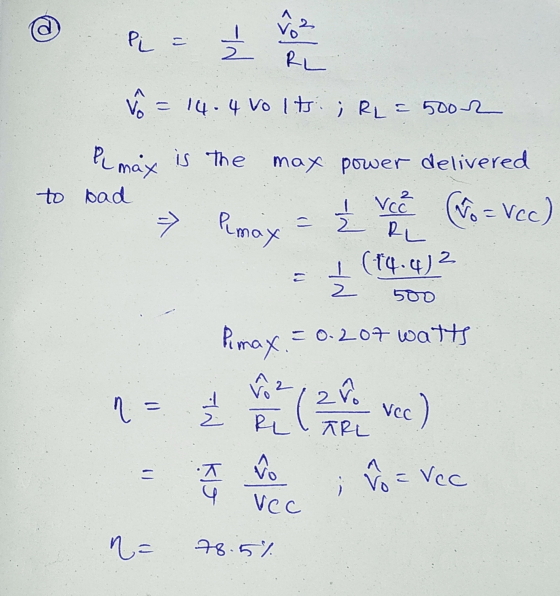
2. Consider a class B BJT output stage with a square wave output voltage of amplitude Vo across a...
 2. Consider a class B BJT output stage with a square wave output voltage of amplitude Vo across a load Ri. and employing power supplies Vss. Neglecting the effects of finite VBE and VCEs (i.e., assume both VBE and VcEsat are negligible small) determine the load power, the supply power, the power conversion efficiency, the maximum attainable power conversion efficiency and the corresponding value of Vo.
2. Consider a class B BJT output stage with a square wave output voltage...
2. Consider a class B BJT output stage with a square wave output voltage of amplitude Vo across a load Ri. and employing power supplies Vss. Neglecting the effects of finite VBE and VCEs (i.e., assume both VBE and VcEsat are negligible small) determine the load power, the supply power, the power conversion efficiency, the maximum attainable power conversion efficiency and the corresponding value of Vo.
2. Consider a class B BJT output stage with a square wave output voltage...
Q2. Calculate the power efficiency and power dissipation Pp of each transistor in the complementary class...
 Q2. Calculate the power efficiency and power dissipation Pp of each transistor in the complementary class B push-pull output stage in Figure 2 ir Vcc 12V and R = 5022. The parameters of the transistors are Bp=hje = 100, VCE(sat) = 0.2V and VBE = 0.7V. (5 Points) BRL VO Floure
 For the emitter follower of Fig. 12.2. let Vcc-10 V, 1-1 00 mA, and R.-100 Ω. If the output voltage is an 8-V-peak sinusoid, find the following: (a) the power delivered to the load; (b) the average power drawn from the supplies: (c) the power-conversion efficiency. Ignore the loss in Qs and R 0 URE 02
For the emitter follower of Fig. 12.2. let Vcc-10 V, 1-1 00 mA, and R.-100 Ω. If the output voltage is an 8-V-peak sinusoid,...
For the emitter follower of Fig. 12.2. let Vcc-10 V, 1-1 00 mA, and R.-100 Ω. If the output voltage is an 8-V-peak sinusoid, find the following: (a) the power delivered to the load; (b) the average power drawn from the supplies: (c) the power-conversion efficiency. Ignore the loss in Qs and R 0 URE 02
For the emitter follower of Fig. 12.2. let Vcc-10 V, 1-1 00 mA, and R.-100 Ω. If the output voltage is an 8-V-peak sinusoid,...
 It is required to design a class B output stage to deliver an average power of 20 W to an 8-Ω load. The power supply is to be selected such that Vcc is about 5 V greater than the peak output voltage. This avoids transistor saturation and the associated nonlinear distortion, and allows for including short-circuit protection circuitry. (The latter will be discussed in Section 12.6.) Determine the supply voltage required the peak current drawn from each supply, the total...
 2. Design an idealized class B output stage, as shown in Figure 2, to deliver an average of 25 W to an 82 speaker. The peak output voltage must be no larger than 80 percent of supply voltages Vcc. Determine: a) The required value of Voc b) The peak current in each transistor c) The power conversion efficiency V+ On Vo ap RL Figure 2
 Page 1. (a) Prove that if the voltage across a resistor Ri is a sine wave with amplitude Vcc, then the average power dissipated during one cycle is given by Vec/2R (b) A Class B BJT output stage is shown in Fig. I. Assume that Vout(t) = Vcc. sin wt; Voe >> VCE(oat); and . Also ignore any crossover distortion effects due to the deddband in the voltage transfer characteristic. Sketch the waveforms for lci(t), Ic2(t) and It(t). (c) Find...
 8.4 a) b) Please solve
Test Your Understanding TYU 8.4 For the common-emitter output stage shown in Figure 8.16(a), let Vcc = 12 V and RL = 1 k12. Assume the transistor Q-point is in the center of the load line. (a) Determine the quiescent power dissipated in the transistor. (b) Assume the sinusoidal output voltage is limited to a 9V peak-to-peak value. Determine (i) the average signal power delivered to the load, (ii) the power conversion efficiency, and (iii)...
8.4 a) b) Please solve
Test Your Understanding TYU 8.4 For the common-emitter output stage shown in Figure 8.16(a), let Vcc = 12 V and RL = 1 k12. Assume the transistor Q-point is in the center of the load line. (a) Determine the quiescent power dissipated in the transistor. (b) Assume the sinusoidal output voltage is limited to a 9V peak-to-peak value. Determine (i) the average signal power delivered to the load, (ii) the power conversion efficiency, and (iii)...
 Class C power amplifier
calculation
(c) A Class C power amplifier shown in Figure-Q4 has a base bias voltage V" = -5V and Vcc = 30V. It is determined that a peak value of 9.8V at 1MHz is required to drive the transistor to its saturation current of 1.8A. Further let the ratio, peak value of the fundamental component to the peak value of the output waveform be approximated by (-0.0072贍+ 4.1e-3.54) × 10-3 where 0c is the conduction angle...
Class C power amplifier
calculation
(c) A Class C power amplifier shown in Figure-Q4 has a base bias voltage V" = -5V and Vcc = 30V. It is determined that a peak value of 9.8V at 1MHz is required to drive the transistor to its saturation current of 1.8A. Further let the ratio, peak value of the fundamental component to the peak value of the output waveform be approximated by (-0.0072贍+ 4.1e-3.54) × 10-3 where 0c is the conduction angle...
 Solve for the over-all Power Gain, Output Power, Quiescent Power, and Efficiency Vee 12V Qa 0, 0.22 pP 10 pF o Ln OkH 00 pF 33 Ω 2 W 100 pF 3 Class C(15pts) 2.1 For a class B amplifier providing a 20-V peak signal to a 16- ohm load (speaker) and a power supply of VCC 30 V, determine the A class C amplifier is driven by a 100 kHz signal. The transistor is on for 2 us, and...
 2. Consider a class B BJT output stage with a square wave output voltage of amplitude Vo across a load Ri. and employing power supplies Vss. Neglecting the effects of finite VBE and VCEs (i.e., assume both VBE and VcEsat are negligible small) determine the load power, the supply power, the power conversion efficiency, the maximum attainable power conversion efficiency and the corresponding value of Vo.
2. Consider a class B BJT output stage with a square wave output voltage...
2. Consider a class B BJT output stage with a square wave output voltage of amplitude Vo across a load Ri. and employing power supplies Vss. Neglecting the effects of finite VBE and VCEs (i.e., assume both VBE and VcEsat are negligible small) determine the load power, the supply power, the power conversion efficiency, the maximum attainable power conversion efficiency and the corresponding value of Vo.
2. Consider a class B BJT output stage with a square wave output voltage...
 Q2. Calculate the power efficiency and power dissipation Pp of each transistor in the complementary class B push-pull output stage in Figure 2 ir Vcc 12V and R = 5022. The parameters of the transistors are Bp=hje = 100, VCE(sat) = 0.2V and VBE = 0.7V. (5 Points) BRL VO Floure
Most questions answered within 3 hours.
-
10. Complete the table below
only using hexadecimal numbers:
AL CODE
EBX
EAX
[EAX]
mov eax,...
asked 2 minutes ago -
trust is best established through the combination of ------and
------- .
1. magnanimity and justice
2....
asked 16 minutes ago -
Blood pressure is normally taken on the upper arm at the level
of the heart. Suppose,...
asked 15 minutes ago -
Suppose that the satellite around the earth has an orbit that is
24 KM larger in...
asked 18 minutes ago -
Calculate the [OH (aq)] in limes which have a [H3O*(aq)] of 1.3 x
10 mol/L
asked 16 minutes ago -
A nozzle with a radius of 0.250 cm is attached to a garden hose
with a...
asked 28 minutes ago -
PLEASE do not use any loops for the program; only recursion is
allowed
4. Write a...
asked 36 minutes ago -
Please help me with me. I did the first part to write the operations but in...
asked 34 minutes ago -
Use Cryptool to find the Cryptographic SHA-1 hash value of the
string "abc". The calculator is...
asked 38 minutes ago -
You are attempting to calculate a firm’s free cash flow to
equity. You know the following...
asked 1 hour ago -
the following reaction occurs in a balloon containing
N2O2 gas
N2O4(g)=2NO2(g)
will the volume of the...
asked 2 hours ago -
answer the questions throughout this program
public class Day implements Comparable {
Private Boolean atWork;...
asked 2 hours ago