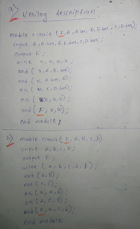
(a) write a Verilog description of the circuit shown below

module Circuit (F, A, A_bar, B, B_bar, C, D_bar); ……….. Endmodule (b) Write a Verilog description of the circuit specified by the following Boolean function:
Z = (A + B’)C’(C + D)
Homework Answers
Add Answer to:
(a) write a Verilog description of the circuit shown below
module Circuit (F, A, A_bar, B,...
HW7.1.1) Which of the Verilog structural descriptions is equivalent to the following Verilog behavioral description? module...
HW7.1.1) Which of the Verilog structural descriptions is equivalent to the following Verilog behavioral description? module hw7_1_1 (x1, x2, x3, f); input x1, x2, x3; output f; assign f = x3 ? x1 : x2; endmodule
HW7.2.3) Which of the Verilog structural descriptions is equivalent to the following Verilog behavioral description? module...
HW7.2.3) Which of the Verilog structural descriptions is equivalent to the following Verilog behavioral description? module hw7_2_3 (x1, x2, x3, f); input x1, x2, x3; output f; always @ (x1, x2, x3) if (x1 == 0) f = x2 & ~x3; else f = ~x2 & x3; endmodule
Draw the circuit corresponding to the Verilog module below. (Do not attempt to simplify the circuit.)...
 Draw the circuit corresponding to the Verilog module below. (Do not attempt to simplify the circuit.) module Circuit A (e, F, G, H); parameter n= 3; input [n-1:0] F, G; input e; output reg [n-1:0] H; integer k; always @ (e, F, G) begin for (k=0; k<n; k=k+1) H[k] = (e | F[k]) & G[k]; end endmodule
Write a test bench to thoroughly test the Verilog module dff_fe_asyn_h. below is the module ddff_fe_asyn_h.code...
Write a test bench to thoroughly test the Verilog module dff_fe_asyn_h. below is the module ddff_fe_asyn_h.code Simulate the circuit using ISim and analyze the resulting waveform. Verilog Code for dff_fe_asyn_h is mentioned below:- //DFF module with asynchronous active high reset with negative edge trigger with clock module dff_fe_asyn_h ( input clock, // Clock Input input reset, // Reset Input input data_in, // Input Data output reg data_out // Output Data ); always @ (negedge clock or posedge reset) // triggers...
why its 4-to-1 mux behavioral? What does the logic circuit represented by the following Verilog module...
 why its 4-to-1 mux behavioral?
What does the logic circuit represented by the following Verilog module do, and what Verilog description style does it use? // My Verilog module #1 module mymodl ( x, d, q) input[1:0] x;input[3:0] d;output q; reg q; wire [1:0] x; wire [3:0] d; always ( x or d) begin case ( x ) 1 : q=d[1]; 2 : g=d[2]; 3 q d[3]; endcase end endmodule
why its 4-to-1 mux behavioral?
What does the logic circuit represented by the following Verilog module do, and what Verilog description style does it use? // My Verilog module #1 module mymodl ( x, d, q) input[1:0] x;input[3:0] d;output q; reg q; wire [1:0] x; wire [3:0] d; always ( x or d) begin case ( x ) 1 : q=d[1]; 2 : g=d[2]; 3 q d[3]; endcase end endmodule
3. (10 Points) RTL Combinational Circuit Design a Draw the schematic for the Verilog code given...
 3. (10 Points) RTL Combinational Circuit Design a Draw the schematic for the Verilog code given below: module abc (a, b, c, d, si, s0); input 31, 30; output a, b, c,d; not (51_, 51), (50_, 0); and (a, s1_, SO_); and (b, s1_, 0); and (c, sl, s0_); and (d, sl, s0); endmodule b. Draw the schematic for the Verilog code given below: module Always_Code input a, b, c, output reg F ); always @(a, b, c) begin F...
Question 3: Realize the circuit below using Verilog. Include a signal “reset_n” for asynchronously clearing the...
 Question 3: Realize the circuit below using Verilog. Include a signal “reset_n” for asynchronously clearing the flip-flop. What type of circuit is this? Complete the following Verilog code. Write a test bench to test it. clk sel module aff (clk, reset_n, sel, q); input clk ; // Declare the inputs and outputs of the module. input reset_n; input sel; output q; reg q; wire D; ; // model the combinational logic assign D= always @( begin if ( else end...
Write a Verilog module that implements the following Boolean equation: f1 = a * b *...
Write a Verilog module that implements the following Boolean equation: f1 = a * b * c' + a * c + b * c Simplify the above expression; write another module to implement it as f2. Write a test bench to check whether f1 and f2 are identical with different values of a, b and c.
Page |3 The function being considered is F(x, y,z)- 20,1,3,4,5,6) 5. Write the Verilog module rep...
 Page |3 The function being considered is F(x, y,z)- 20,1,3,4,5,6) 5. Write the Verilog module representing the minimized function in column I (with primitives). module mod ( outhut
Page |3 The function being considered is F(x, y,z)- 20,1,3,4,5,6) 5. Write the Verilog module representing the minimized function in column I (with primitives). module mod ( outhut
Page |3 The function being considered is F(x, y,z)- 20,1,3,4,5,6) 5. Write the Verilog module representing the minimized function in column I (with primitives). module mod ( outhut
Page 13 The function being considered is F(x, y,z) 20,1,3,4,5,6) S. Write the Verilog module repr...
 Page 13 The function being considered is F(x, y,z) 20,1,3,4,5,6) S. Write the Verilog module representing the minimized function in column I (with primitives)
Page 13 The function being considered is F(x, y,z) 20,1,3,4,5,6) S. Write the Verilog module representing the minimized function in column I (with primitives)
Page 13 The function being considered is F(x, y,z) 20,1,3,4,5,6) S. Write the Verilog module representing the minimized function in column I (with primitives)
 Draw the circuit corresponding to the Verilog module below. (Do not attempt to simplify the circuit.) module Circuit A (e, F, G, H); parameter n= 3; input [n-1:0] F, G; input e; output reg [n-1:0] H; integer k; always @ (e, F, G) begin for (k=0; k<n; k=k+1) H[k] = (e | F[k]) & G[k]; end endmodule
 why its 4-to-1 mux behavioral?
What does the logic circuit represented by the following Verilog module do, and what Verilog description style does it use? // My Verilog module #1 module mymodl ( x, d, q) input[1:0] x;input[3:0] d;output q; reg q; wire [1:0] x; wire [3:0] d; always ( x or d) begin case ( x ) 1 : q=d[1]; 2 : g=d[2]; 3 q d[3]; endcase end endmodule
why its 4-to-1 mux behavioral?
What does the logic circuit represented by the following Verilog module do, and what Verilog description style does it use? // My Verilog module #1 module mymodl ( x, d, q) input[1:0] x;input[3:0] d;output q; reg q; wire [1:0] x; wire [3:0] d; always ( x or d) begin case ( x ) 1 : q=d[1]; 2 : g=d[2]; 3 q d[3]; endcase end endmodule
 3. (10 Points) RTL Combinational Circuit Design a Draw the schematic for the Verilog code given below: module abc (a, b, c, d, si, s0); input 31, 30; output a, b, c,d; not (51_, 51), (50_, 0); and (a, s1_, SO_); and (b, s1_, 0); and (c, sl, s0_); and (d, sl, s0); endmodule b. Draw the schematic for the Verilog code given below: module Always_Code input a, b, c, output reg F ); always @(a, b, c) begin F...
 Question 3: Realize the circuit below using Verilog. Include a signal “reset_n” for asynchronously clearing the flip-flop. What type of circuit is this? Complete the following Verilog code. Write a test bench to test it. clk sel module aff (clk, reset_n, sel, q); input clk ; // Declare the inputs and outputs of the module. input reset_n; input sel; output q; reg q; wire D; ; // model the combinational logic assign D= always @( begin if ( else end...
 Page |3 The function being considered is F(x, y,z)- 20,1,3,4,5,6) 5. Write the Verilog module representing the minimized function in column I (with primitives). module mod ( outhut
Page |3 The function being considered is F(x, y,z)- 20,1,3,4,5,6) 5. Write the Verilog module representing the minimized function in column I (with primitives). module mod ( outhut
Page |3 The function being considered is F(x, y,z)- 20,1,3,4,5,6) 5. Write the Verilog module representing the minimized function in column I (with primitives). module mod ( outhut
 Page 13 The function being considered is F(x, y,z) 20,1,3,4,5,6) S. Write the Verilog module representing the minimized function in column I (with primitives)
Page 13 The function being considered is F(x, y,z) 20,1,3,4,5,6) S. Write the Verilog module representing the minimized function in column I (with primitives)
Page 13 The function being considered is F(x, y,z) 20,1,3,4,5,6) S. Write the Verilog module representing the minimized function in column I (with primitives)
Most questions answered within 3 hours.
-
A χ2-curve, looking at the relationship between age and hours
spent working at an office per...
asked 12 minutes ago -
The pH of a sample of water from a river is 5.0. A
sample of effluent from...
asked 57 minutes ago -
At the beginning of the period, the Fabricating Department
budgeted direct labor of $136,500 and equipment...
asked 1 hour ago -
Please answer all
____ 28. Rent control is usually
justified on the grounds that it protects...
asked 1 hour ago -
PARTS A-D HAVE BEEN ANSWERED. WAS TOLD TO REPOST. ONLY ANSWER
PARTS E and F.
A...
asked 1 hour ago -
2) You are given the task of finding a representation for a
circle in a drawing...
asked 2 hours ago -
STUDY QUESTION: Does use of diet drug fen-phen
(fenfluramine-phentermine) cause valvular heart disease?
HINT: Valvular heart...
asked 2 hours ago -
1. An object weighing 40 N rests on a surface. The coefficient
of friction is 0.35....
asked 3 hours ago -
Investor company owns 35% of investee company voting stock and
accounts for the investment under the...
asked 5 hours ago -
The number of major faults on a randomly chosen 1 km stretch of
highway has a...
asked 5 hours ago -
Consider the competitive environment of Starbuck's, Progressive
Insurance, a manufacturing firm with low turnover, or a...
asked 6 hours ago -
3. Gains from trade
Consider two neighbouring island countries called Euphoria and
Contente. They each have...
asked 8 hours ago