
Homework Answers
SOLUTION:

PLEASE GIVE ME LIKE..ITS HELP ME TO WRITE MORE QUESTIONS..THANK YOU..
Add Answer to:
In the circuit shown, a center-tapped transformer is used to create a full- wave center-tapped configuration....
3. Consider the full-wave bridge rectifier circuit shown below. The full-wave bridge is made using silicon...
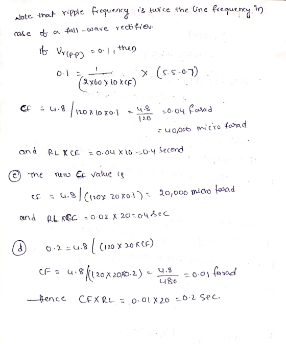
 3. Consider the full-wave bridge rectifier circuit shown below. The full-wave bridge is made using silicon diodes. 120V 15V 120 V(ms) n 60 Hz 752 Vout a. Find the maximum value of VoUT, and the voltage rating for the capacitor assuming a 50% margin of safety. b. Choose the capacitance of the filter capacitor for a peak-to-peak ripple of 1V, and determine the corresponding peak diode current. What is the frequency of the ripple voltage? c. Now suppose the filter...
Consider the single-phase full-wave rectifier circuit shown below with a sinusoidal input vs 120 Vrms at...
 Consider the single-phase full-wave rectifier circuit shown below with a sinusoidal input vs 120 Vrms at 60 Hz and a load R= 250 TiD DAZ 40 AD AD ww D (a) (b) Consider adding a filter capacitor to the full-wave rectifier in Problem 3 to reduce the output ripple (a) Calculate the minimum value of capacitance required to reduce the output voltage ripple to 1 % of the average value (b) Calculate the average output current (c) Calculate the average...
Question 2 of 9 Question 2 12 points Saved A full-wave bridge rectifier has 60 Hz...
 Question 2 of 9 Question 2 12 points Saved A full-wave bridge rectifier has 60 Hz input signal and the voltage signal applied at its input (secondary voltage of transformer) is at 12V rms. If the voltage drop across a diode is 0.6V and the load resistance is 10 kOhms, determine the required capacitance value to limit the ripple value to 0.1V. Choose the value closest the what you have found. 41.7 microfarad 13.14 microfarad 417 microfarad 131.4 microfarad -...
A full-wave diode rectifier supplies a 30Ω resistive load from a 400Hz, 110V single-phase AC supply....
A full-wave diode rectifier supplies a 30Ω resistive load from a 400Hz, 110V single-phase AC supply. A capacitor is connected in parallel with the load. Calculate the capacitance required if the maximum peak-to-peak voltage ripple across the resistor is to be restricted to 10V. You may assume that the RC product of the resistance and capacitance will be significantly greater than the period of the AC waveform. State any other assumptions made.
Question 1 (25 marks) a) A full wave rectifier has 40V peak secondary voltage, 2,000uF capacitor...
 Question 1 (25 marks) a) A full wave rectifier has 40V peak secondary voltage, 2,000uF capacitor and 1022 load. You may take the line frequency as 50Hz and voltage drop across a diode as 0.7V. i. Calculate the peak dc voltage (VA). (2 marks) ii. Calculate the dc load voltage (Vdcloed). (4 marks) iii. Calculate the ripple voltage (AVLoad). (4 marks) b) The capacitance, inductance and load resistance of a Buck step-down dc-to-dc converter are 1.0uF, 10uH and 20.022 respectively....
Design a FULL WAVE BRIDGE RECTIFIER circuit that will: Take 120volts ac, 60 hz, sinusoidal wavef...
Design a FULL WAVE BRIDGE RECTIFIER circuit that will: Take 120volts ac, 60 hz, sinusoidal waveform from the wall power and convert it to a “regulated” dc value giving 15 volts +, - 1.0 volts across a 1200-ohm output load resistor with no more than 2% ripple voltage, all at a total component parts cost of less than $175.00 (US$). Your design process/ analysis is to be conducted by hand. Consider for this design task: Assume an ideal transformer and...
Design a FULL WAVE BRIDGE RECTIFIER circuit that will: Take 120volts ac, 60 hz, sinusoidal waveform...
 Design a FULL WAVE BRIDGE RECTIFIER circuit that will:
Take 120volts ac, 60 hz, sinusoidal waveform and convert
it to a “regulated “dc value
giving 12 volts +, - 1 volt across a 2000-ohm output
load resistor with no more than 2%
ripple voltage.
You may assume:
a. An ideal power transformer as discussed in class.
b. For hand computations, you must assume a diode given by
Figure 4.8 page 185.
c. A filter capacitor sized per the textbook equation...
Design a FULL WAVE BRIDGE RECTIFIER circuit that will:
Take 120volts ac, 60 hz, sinusoidal waveform and convert
it to a “regulated “dc value
giving 12 volts +, - 1 volt across a 2000-ohm output
load resistor with no more than 2%
ripple voltage.
You may assume:
a. An ideal power transformer as discussed in class.
b. For hand computations, you must assume a diode given by
Figure 4.8 page 185.
c. A filter capacitor sized per the textbook equation...
32. A transformer is to be designed to increase the 30 kV-rms output of a generator...
 32. A transformer is to be designed to increase the 30 kV-rms output of a generator to the transmission-line voltage of 345 kV-om. If the primary winding has 80 turns, how many turns must the secondary have? b. 70 c. 920 d. 9200 e 12 33. The primary winding of an electric train transformer has 400 turns and the Secondary has 50. If the input voltage is 120V(rms) what is the output voltage? a. 15 V (rms) b. 30 Vrms)...
ll capace, expressed in oks. They 9. The opposition offered to the non offered to the...
 ll capace, expressed in oks. They 9. The opposition offered to the non offered to the flow of a C alensis XE. 1. Inductive Reactance 2. Capacitive Reactance 3. Impedance 4. Resistance 10. The opposition offered to the The opposition offered to the flow of an alteratine curenty inductance, expressed in ons. The symbol for characteristic is XL. 1. Inductive Reactance 2. Capacitive Reactance 3. Impedance when a voltage 11. What is the basic unit of capacitance? Example: A capacitor...
A common source amplifier circuit based on a single n-channel MOSFET is shown in Figure 4b. Assume that the transconductance gm-60 mS (equivalent to mA/ V) and drain source resistance, os,...
 A common source amplifier circuit based on a single n-channel MOSFET is shown in Figure 4b. Assume that the transconductance gm-60 mS (equivalent to mA/ V) and drain source resistance, os, is so large it may be neglected. 0) Calculate the open circuit voltage gain Av Yout/ Vis. i) The amplifier has a load of 10 k2. Determine the current gain Va. = 12 V 150k 4k3 Vout Vin 200k GND = 0 V Figure 4b a) State the name...
 3. Consider the full-wave bridge rectifier circuit shown below. The full-wave bridge is made using silicon diodes. 120V 15V 120 V(ms) n 60 Hz 752 Vout a. Find the maximum value of VoUT, and the voltage rating for the capacitor assuming a 50% margin of safety. b. Choose the capacitance of the filter capacitor for a peak-to-peak ripple of 1V, and determine the corresponding peak diode current. What is the frequency of the ripple voltage? c. Now suppose the filter...
 Consider the single-phase full-wave rectifier circuit shown below with a sinusoidal input vs 120 Vrms at 60 Hz and a load R= 250 TiD DAZ 40 AD AD ww D (a) (b) Consider adding a filter capacitor to the full-wave rectifier in Problem 3 to reduce the output ripple (a) Calculate the minimum value of capacitance required to reduce the output voltage ripple to 1 % of the average value (b) Calculate the average output current (c) Calculate the average...
 Question 2 of 9 Question 2 12 points Saved A full-wave bridge rectifier has 60 Hz input signal and the voltage signal applied at its input (secondary voltage of transformer) is at 12V rms. If the voltage drop across a diode is 0.6V and the load resistance is 10 kOhms, determine the required capacitance value to limit the ripple value to 0.1V. Choose the value closest the what you have found. 41.7 microfarad 13.14 microfarad 417 microfarad 131.4 microfarad -...
 Question 1 (25 marks) a) A full wave rectifier has 40V peak secondary voltage, 2,000uF capacitor and 1022 load. You may take the line frequency as 50Hz and voltage drop across a diode as 0.7V. i. Calculate the peak dc voltage (VA). (2 marks) ii. Calculate the dc load voltage (Vdcloed). (4 marks) iii. Calculate the ripple voltage (AVLoad). (4 marks) b) The capacitance, inductance and load resistance of a Buck step-down dc-to-dc converter are 1.0uF, 10uH and 20.022 respectively....
 Design a FULL WAVE BRIDGE RECTIFIER circuit that will:
Take 120volts ac, 60 hz, sinusoidal waveform and convert
it to a “regulated “dc value
giving 12 volts +, - 1 volt across a 2000-ohm output
load resistor with no more than 2%
ripple voltage.
You may assume:
a. An ideal power transformer as discussed in class.
b. For hand computations, you must assume a diode given by
Figure 4.8 page 185.
c. A filter capacitor sized per the textbook equation...
Design a FULL WAVE BRIDGE RECTIFIER circuit that will:
Take 120volts ac, 60 hz, sinusoidal waveform and convert
it to a “regulated “dc value
giving 12 volts +, - 1 volt across a 2000-ohm output
load resistor with no more than 2%
ripple voltage.
You may assume:
a. An ideal power transformer as discussed in class.
b. For hand computations, you must assume a diode given by
Figure 4.8 page 185.
c. A filter capacitor sized per the textbook equation...
 32. A transformer is to be designed to increase the 30 kV-rms output of a generator to the transmission-line voltage of 345 kV-om. If the primary winding has 80 turns, how many turns must the secondary have? b. 70 c. 920 d. 9200 e 12 33. The primary winding of an electric train transformer has 400 turns and the Secondary has 50. If the input voltage is 120V(rms) what is the output voltage? a. 15 V (rms) b. 30 Vrms)...
 ll capace, expressed in oks. They 9. The opposition offered to the non offered to the flow of a C alensis XE. 1. Inductive Reactance 2. Capacitive Reactance 3. Impedance 4. Resistance 10. The opposition offered to the The opposition offered to the flow of an alteratine curenty inductance, expressed in ons. The symbol for characteristic is XL. 1. Inductive Reactance 2. Capacitive Reactance 3. Impedance when a voltage 11. What is the basic unit of capacitance? Example: A capacitor...
 A common source amplifier circuit based on a single n-channel MOSFET is shown in Figure 4b. Assume that the transconductance gm-60 mS (equivalent to mA/ V) and drain source resistance, os, is so large it may be neglected. 0) Calculate the open circuit voltage gain Av Yout/ Vis. i) The amplifier has a load of 10 k2. Determine the current gain Va. = 12 V 150k 4k3 Vout Vin 200k GND = 0 V Figure 4b a) State the name...
Most questions answered within 3 hours.
-
Are there such things as microscopic multicellular animal
parasites? If so, please give examples.
asked 25 minutes ago -
1. What two structures in the ear are involved in your
sense of balance and in...
asked 12 minutes ago -
Two ice skaters suddenly push off against one another starting
from a stationary position. The 45...
asked 13 minutes ago -
What is the Larmor frequency for a proton in a magnetic field of
B0 = 14.0...
asked 14 minutes ago -
Problem 03.019 Annual Worth Calculations
Find the value of x that makes the equivalent annual
worth...
asked 30 minutes ago -
Under common law, right of survivorship was automatically a
feature of which type of co-tenancy?
a....
asked 26 minutes ago -
At 1 bar, how much energy is required to heat 61.0 g of H2O(s)
at −12.0...
asked 47 minutes ago -
Find the mixed-strategy equilibrium to the Battle of the sexes
game in Figure 5.1 below
Hockey...
asked 49 minutes ago -
Use the following information to answer the next three
questions.
QUESTION 5
As of today, the...
asked 54 minutes ago -
Using the specific identification method: Date Units purchased
Cost per unit Ending inventory March 1 15...
asked 57 minutes ago -
PLEASE HELP, NO ONE IS ANSWERING MY QUESTION AND IT IS SUE TODAY
WORTH 20% OF...
asked 1 hour ago -
α = 0.0007889 T, I = 2.9 A
Other Magnetic Fields: First, based on your
value...
asked 1 hour ago