
Homework Answers

Add Answer to:
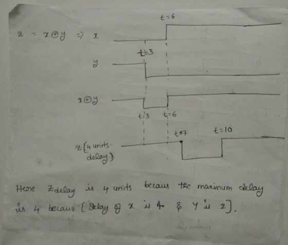
4. [20 points) Draw a timing diagram with causality arrows for b, w, x, y, and...
Simplify the circuit below to obtain the most simplified SOP implementation using any method. Dra...
 Simplify the circuit below to obtain the most simplified SOP implementation using any method. Draw a timing diagram for the truth table of the circuit below. Assume each input combination lasts for 20 ns and the propagation delay from the input of the circuit to the output is a total of 10ns. See slide 61 of Chapter 2 slides for an example of an "ideal but with delay" timing diagram for the output. (12 pts) 1. 10 Find the critical...
I have the timing diagram down but I am still fuzzy on these two questions. 1....
 I have the timing diagram down but I am still fuzzy on these two
questions.
1. What is the delay of the longest circuit path?
2. What is the delay of the shortest circuit path?
Indicate the delays as number of gate delays. Make sure to consider
the entire circuit
for finding the shortest/longest circuit path. These delays are not
tied to the specific
input change that was indicated for the timing diagram, but can be
any input change.
.......
I have the timing diagram down but I am still fuzzy on these two
questions.
1. What is the delay of the longest circuit path?
2. What is the delay of the shortest circuit path?
Indicate the delays as number of gate delays. Make sure to consider
the entire circuit
for finding the shortest/longest circuit path. These delays are not
tied to the specific
input change that was indicated for the timing diagram, but can be
any input change.
.......
1) Draw the diagram of XOR gate using AND, OR and NOT gates only 2) Draw...
1) Draw the diagram of XOR gate using AND, OR and NOT gates only 2) Draw the diagram of this function (x,y) = (x’y + xy’ + x’y’) using NOT, AND gates only 3) Draw the diagram of this function (x,y,z,w) = (x’ + y’).(z + w) using 2 input NAND gates only Draw the diagram of this function (x,y,z) = xy’z using 2 input NAND gates only.
Question 5. Finish the timing diagram for V and Z signals of the next circuit with...
 Question 5. Finish the timing diagram for V and Z signals of the next circuit with delays of AND beside OR gates as shown on the circuit. AND gate delay5ns and OR gate delay 10 ns 5 ns 10 ns - Z W X Y Z 10 15 20 25 30 35 40 45 50 55 (ns) 0 5 Question 6. Consider the following function F (A, B, C, D) A'B' + A'C + BC A. Find all static-0 hazards....
microprocessors,,pls help.. 1. (3 Points) Draw a timing diagram similar to the 'practical' case of figure...
 microprocessors,,pls help..
1. (3 Points) Draw a timing diagram similar to the 'practical' case of figure 5, below, for the case where signal Ao makes its transition first. Note: For each timing diagram that you draw, be sure that subsequent events appear to the right of causative events, and show causality arrows. 3.1 Glitch pulses Consider the one-bit adder circuit of figure 4. This circuit is called a one-bit (binary) adder because output signal So is the sum of input...
microprocessors,,pls help..
1. (3 Points) Draw a timing diagram similar to the 'practical' case of figure 5, below, for the case where signal Ao makes its transition first. Note: For each timing diagram that you draw, be sure that subsequent events appear to the right of causative events, and show causality arrows. 3.1 Glitch pulses Consider the one-bit adder circuit of figure 4. This circuit is called a one-bit (binary) adder because output signal So is the sum of input...
I need help drawing the Timing diagram and Finding the Hazards. (A) Draw the timing dlagram for the circuit belov If B changes from 1 to 0 at 20ns (assume B was 1 already before the time 0 sec.) Assu...
 I need help drawing the Timing diagram and Finding the
Hazards.
(A) Draw the timing dlagram for the circuit belov If B changes from 1 to 0 at 20ns (assume B was 1 already before the time 0 sec.) Assume A1andCat any time, including time <0 sec.) and each inverter or gate has a propagation delay of 10ns. Delo 0 10 20 30 4050 60 70Time (ns) B) Draw the timing diagram for the circuit below if C changes from...
I need help drawing the Timing diagram and Finding the
Hazards.
(A) Draw the timing dlagram for the circuit belov If B changes from 1 to 0 at 20ns (assume B was 1 already before the time 0 sec.) Assume A1andCat any time, including time <0 sec.) and each inverter or gate has a propagation delay of 10ns. Delo 0 10 20 30 4050 60 70Time (ns) B) Draw the timing diagram for the circuit below if C changes from...
The following logic function is given as a sum of minterms F(W,X,Y,Z) = ∑W,X,Y,Z(2,7,10,13,14) + d(5,6,15)...
The following logic function is given as a sum of minterms F(W,X,Y,Z) = ∑W,X,Y,Z(2,7,10,13,14) + d(5,6,15) a) Draw the K-map for the given function F. b) What is the minimized SOP equation? c) Give all input pairs in the form of WXYZ where a transition between them would create a timing hazard. d) Draw the timing diagram showing the hazard for one of the cases. Assume ALL gate delays are equal. e) Provide the expression of an equivalent logic function...
b) For the circuit below, draw the timing diagram for outputs X and Y for the...
 b) For the circuit below, draw the timing diagram for outputs X and Y for the CLK signal shown below. Note that the flip-flops are negative-edge-triggered. Ignore the propagation delays. Assume X=Y=0 at the start. (6 Points) LO 7x CLK CLK d oo Loy CLK
Provide a breadboard schematic and expected output timing diagram showing how your circuit should behave Using...
Provide a breadboard schematic and expected output timing diagram showing how your circuit should behave Using any combination of the following components: 2 74HC00 quad 2-input NAND gate IC 1 74HC04 hex inverter IC 2 74HC08 quad 2-input AND gate IC 2 74HC32 quad 2-input OR gate IC 3 74HC74 dual D positive edge triggered flip-flop IC 1 74HC86 quad 2-input XOR gate IC 1 74HC157 quad 2-input multiplexer IC 1 CD74HCT390 dual decade counter IC 1 71256 32Kx8 SRAM...
Draw the gate level circuit schematic of a D flip-flop and a T flip-flop based on the cross-coupled NAND latch. Briefly discuss the timing behavior of a D flip-flop, a T flip-flop and a latch. (a) (8...
 Draw the gate level circuit schematic of a D flip-flop and a T flip-flop based on the cross-coupled NAND latch. Briefly discuss the timing behavior of a D flip-flop, a T flip-flop and a latch. (a) (8 Marks) circuit has three inputs, S, C and C2. S is the control input. When S-O, the circuit behaves like a D flip-flop, and when S-1, the circuit behaves like a T flip-flop. The input characteristics of the circuit are tabulated in Table...
 Simplify the circuit below to obtain the most simplified SOP implementation using any method. Draw a timing diagram for the truth table of the circuit below. Assume each input combination lasts for 20 ns and the propagation delay from the input of the circuit to the output is a total of 10ns. See slide 61 of Chapter 2 slides for an example of an "ideal but with delay" timing diagram for the output. (12 pts) 1. 10 Find the critical...
 I have the timing diagram down but I am still fuzzy on these two
questions.
1. What is the delay of the longest circuit path?
2. What is the delay of the shortest circuit path?
Indicate the delays as number of gate delays. Make sure to consider
the entire circuit
for finding the shortest/longest circuit path. These delays are not
tied to the specific
input change that was indicated for the timing diagram, but can be
any input change.
.......
I have the timing diagram down but I am still fuzzy on these two
questions.
1. What is the delay of the longest circuit path?
2. What is the delay of the shortest circuit path?
Indicate the delays as number of gate delays. Make sure to consider
the entire circuit
for finding the shortest/longest circuit path. These delays are not
tied to the specific
input change that was indicated for the timing diagram, but can be
any input change.
.......
 Question 5. Finish the timing diagram for V and Z signals of the next circuit with delays of AND beside OR gates as shown on the circuit. AND gate delay5ns and OR gate delay 10 ns 5 ns 10 ns - Z W X Y Z 10 15 20 25 30 35 40 45 50 55 (ns) 0 5 Question 6. Consider the following function F (A, B, C, D) A'B' + A'C + BC A. Find all static-0 hazards....
 microprocessors,,pls help..
1. (3 Points) Draw a timing diagram similar to the 'practical' case of figure 5, below, for the case where signal Ao makes its transition first. Note: For each timing diagram that you draw, be sure that subsequent events appear to the right of causative events, and show causality arrows. 3.1 Glitch pulses Consider the one-bit adder circuit of figure 4. This circuit is called a one-bit (binary) adder because output signal So is the sum of input...
microprocessors,,pls help..
1. (3 Points) Draw a timing diagram similar to the 'practical' case of figure 5, below, for the case where signal Ao makes its transition first. Note: For each timing diagram that you draw, be sure that subsequent events appear to the right of causative events, and show causality arrows. 3.1 Glitch pulses Consider the one-bit adder circuit of figure 4. This circuit is called a one-bit (binary) adder because output signal So is the sum of input...
 I need help drawing the Timing diagram and Finding the
Hazards.
(A) Draw the timing dlagram for the circuit belov If B changes from 1 to 0 at 20ns (assume B was 1 already before the time 0 sec.) Assume A1andCat any time, including time <0 sec.) and each inverter or gate has a propagation delay of 10ns. Delo 0 10 20 30 4050 60 70Time (ns) B) Draw the timing diagram for the circuit below if C changes from...
I need help drawing the Timing diagram and Finding the
Hazards.
(A) Draw the timing dlagram for the circuit belov If B changes from 1 to 0 at 20ns (assume B was 1 already before the time 0 sec.) Assume A1andCat any time, including time <0 sec.) and each inverter or gate has a propagation delay of 10ns. Delo 0 10 20 30 4050 60 70Time (ns) B) Draw the timing diagram for the circuit below if C changes from...
 b) For the circuit below, draw the timing diagram for outputs X and Y for the CLK signal shown below. Note that the flip-flops are negative-edge-triggered. Ignore the propagation delays. Assume X=Y=0 at the start. (6 Points) LO 7x CLK CLK d oo Loy CLK
 Draw the gate level circuit schematic of a D flip-flop and a T flip-flop based on the cross-coupled NAND latch. Briefly discuss the timing behavior of a D flip-flop, a T flip-flop and a latch. (a) (8 Marks) circuit has three inputs, S, C and C2. S is the control input. When S-O, the circuit behaves like a D flip-flop, and when S-1, the circuit behaves like a T flip-flop. The input characteristics of the circuit are tabulated in Table...
Most questions answered within 3 hours.
-
I need to write a research paper and work cited about this
topic: The United States...
asked 5 minutes ago -
Hello! I was wondering if I could have some help?
If the vapor pressure of carvone...
asked 27 minutes ago -
An economist wants to estimate the mean per capita income (in
thousands of dollars) for a...
asked 46 minutes ago -
What would be the input/output characteristic of a circuit
obtained by putting two of your 2's-complementers...
asked 45 minutes ago -
In Drosophila, the transition from the syncytial blastoderm
stage to the cellular blastoderm stage is a...
asked 1 hour ago -
Project management question:
Name 3 different types of resources (hint: humans are one
type)
asked 1 hour ago -
Consider the following reaction: C 2H 2( g) + 2H 2( g) C 2H 6(
g)...
asked 1 hour ago -
Consider a 1.0 L buffer containing 0.092 mol L-1 HCOOH and 0.100
mol L-1 HCOO-. What...
asked 1 hour ago -
Koch Realty has owned a vacant land with a FMV of
$775,000 and an adjusted basis...
asked 1 hour ago -
It is estimated 29% of all adults in United States invest in
stocks and that 85%...
asked 1 hour ago -
What does a 2-sided p value of 0.04 mean? (I am not asking if it
is...
asked 2 hours ago -
A parallel-plate capacitor is made from two aluminum-foil
sheets, each 7.8 cmcm wide and 5.1 mmlong....
asked 2 hours ago