
Homework Answers
Add Answer to:
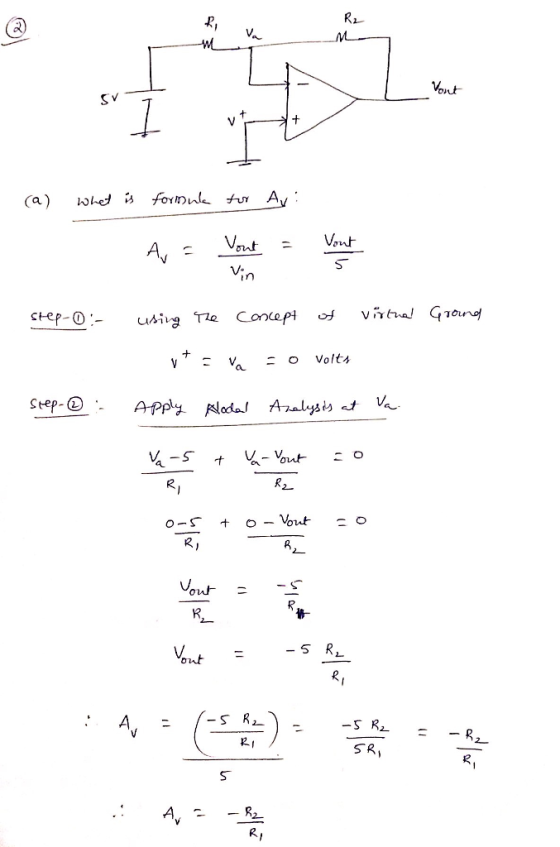
Problem 2. For the following circuit: R1 R2 Va OPAMP Vout OUT 0 (a) What is...
Problem # 3 For the summing opamp circuit, assume that the opamp is powered with +15V and-15V. Th...
 Problem # 3 For the summing opamp circuit, assume that the opamp is powered with +15V and-15V. The input voltages are VI and V2 and the output voltage is Vout. Rf 15 V U1 R1 R2 Vout 741 V2 (A -15 V 1. Find the relation between the output Vout and the inputs VI and V2 2. Assume that RI-2kS2, R2-3 ㏀ and Rf-6kS2, Vin is a sinewave with viinpp-2V, V2DC- IV, plot Vin() and Vout(0) 3. Assume that you...
For the circuit shown below, design the values of R1 and R2 that will cause Vout-6 Vif VIv-9 V. If the resistors you chose have a tolerance of 1 %, what is the maximum and minimum values of Vout? Des...
 For the circuit shown below, design the values of R1 and R2 that will cause Vout-6 Vif VIv-9 V. If the resistors you chose have a tolerance of 1 %, what is the maximum and minimum values of Vout? Design R3 so that the LED will be properly lit, if IF=10 mA, VF-3 V and Vout-6 V Design equations from the data sheet: VOUT-1.25%(1+R2 R1) U1 OUT ININLT OUT R3 R1 V1 (R3) R1) ADJ LT317A D1 IN) R2 (R2)...
3-F) b. Vout = 0.99 Vin 3-E) For the following circuit, with Ri 18 k2, R2...
 3-F) b. Vout = 0.99 Vin
3-E) For the following circuit, with Ri 18 k2, R2 15 k(2, R6 = 40 kQ, V,-10 V, and V,-7 V, find: 22 k2, R 30 k2, R4 20 kQ, Rs- a) the current through Ri, R3, & R6 b) the voltage across R2, R4, & Rs Rs V, 3-F) For the following circuit, what is Vout in terms of Vin for each case? a) R1-100 ?, R2-1 k(2, and R3 = 1.0 M(2...
3-F) b. Vout = 0.99 Vin
3-E) For the following circuit, with Ri 18 k2, R2 15 k(2, R6 = 40 kQ, V,-10 V, and V,-7 V, find: 22 k2, R 30 k2, R4 20 kQ, Rs- a) the current through Ri, R3, & R6 b) the voltage across R2, R4, & Rs Rs V, 3-F) For the following circuit, what is Vout in terms of Vin for each case? a) R1-100 ?, R2-1 k(2, and R3 = 1.0 M(2...
Find V out Vout- For the following problem, assume that all op-amps are ideal C. R2...
 Find V out
Vout- For the following problem, assume that all op-amps are ideal C. R2 R1 Vout 10 kn
Find V out
Vout- For the following problem, assume that all op-amps are ideal C. R2 R1 Vout 10 kn
For the circuit shown below: In terms of Vo, R1, R2, R3, R4, C1, t, and s what is the time domain...
 For the circuit shown below: In terms of Vo, R1, R2, R3, R4, C1, t, and s what is the time domain equation for the voltage at node out? Preview In terms of Vo, R1, R2, ,R3, R4, C1, t, and s what is the s-domain equation for voltage at node out? In terms of Vo, RI, R2, R3, R4, CI, t, and s what is the equation for τ? If the voltage V1 at time-0 is 1 V R1-1...
V1 = 8 (V) Problem 1 R1 = 8 (0) V2 = 26 (V) VA =...
 V1 = 8 (V) Problem 1 R1 = 8 (0) V2 = 26 (V) VA = 28 (V) V3 = 20 (V) Using Kirchhoff's rules in the circuit of image, A- Calculate the current in the circuit. B- Show the direction current in the circuit. C- Calculate the voltage across resistor R1 D- Calculate the power delivered to R2 E After 15 minutes of working of circuit, how much energy is delivered to resistor Rı? R2 = 7(0)
2. In the circuit below, R1 = 10k, R2 : magnitude is applied to the input....
 2. In the circuit below, R1 = 10k, R2 : magnitude is applied to the input. Find V(t) at the output and sketch it. Your sketch should be quantitatively correct, that is, it should have labeled V and t axes. Strongly suggested: solve by first finding the Thévenin equivalent of the source voltage and resistor network. 20k and C = 0.1µF. At t = 0, a step function of 10 V Input (problem 3) R, 10V- IN R2 C, OUT...
For the electrical circuit below, let R1=30 Ohms, R2=15 Ohms, R3=10 Ohms, R4=20 Ohms, C=0.1 F...
 For the electrical circuit below, let R1=30 Ohms, R2=15 Ohms,
R3=10 Ohms, R4=20 Ohms, C=0.1 F and Vin=10V and complete the
following.
For the electrical circuit below, let R1 = 30 12, R2 = 152, R3 = 102, R1 = 20 2, C =0.1 F and Vin = 10V and complete the following. a) Use circuit analysis to derive the differential equation for the capacitor voltage, V.(t). b) Find the solution for V«(t) and sketch it for t=0, t and...
For the electrical circuit below, let R1=30 Ohms, R2=15 Ohms,
R3=10 Ohms, R4=20 Ohms, C=0.1 F and Vin=10V and complete the
following.
For the electrical circuit below, let R1 = 30 12, R2 = 152, R3 = 102, R1 = 20 2, C =0.1 F and Vin = 10V and complete the following. a) Use circuit analysis to derive the differential equation for the capacitor voltage, V.(t). b) Find the solution for V«(t) and sketch it for t=0, t and...
For the circuit shown below: Preview In terms of Vo, R1, R2, R3, R4 C1, t, and s what is the time domain equation for the voltage at node out? Preview and s what is the s-domain equation the voltage...
 For the circuit shown below: Preview In terms of Vo, R1, R2, R3, R4 C1, t, and s what is the time domain equation for the voltage at node out? Preview and s what is the s-domain equation the voltage at node out? In terms of Vo, RI, R2, R3,R4, C1, t, Preview and s what is the equation for τ? In terms ofVo, RI, R2, R3, R4, Cl, t, Ifthe voltage V1 at time-0 is 3 V RI=4 kQ,...
Recall the Offset Nulling Circuit that you used to zero out the offset of the LM741 OpAmp in L200...
 . please help me from a to
e
Recall the Offset Nulling Circuit that you used to zero out the offset of the LM741 OpAmp in L2002B, shown in Figure 1(a). An external 10 k2 potentiometer was applied across the emitter terminals of the current mirror formed by Q5 and Q6 in Figure 1(b), which can be thought of as making an adjustment to collector currents Ics and Ics such that Ics-Ics exactly A simplified version of that current mirror...
. please help me from a to
e
Recall the Offset Nulling Circuit that you used to zero out the offset of the LM741 OpAmp in L2002B, shown in Figure 1(a). An external 10 k2 potentiometer was applied across the emitter terminals of the current mirror formed by Q5 and Q6 in Figure 1(b), which can be thought of as making an adjustment to collector currents Ics and Ics such that Ics-Ics exactly A simplified version of that current mirror...
 Problem # 3 For the summing opamp circuit, assume that the opamp is powered with +15V and-15V. The input voltages are VI and V2 and the output voltage is Vout. Rf 15 V U1 R1 R2 Vout 741 V2 (A -15 V 1. Find the relation between the output Vout and the inputs VI and V2 2. Assume that RI-2kS2, R2-3 ㏀ and Rf-6kS2, Vin is a sinewave with viinpp-2V, V2DC- IV, plot Vin() and Vout(0) 3. Assume that you...
 For the circuit shown below, design the values of R1 and R2 that will cause Vout-6 Vif VIv-9 V. If the resistors you chose have a tolerance of 1 %, what is the maximum and minimum values of Vout? Design R3 so that the LED will be properly lit, if IF=10 mA, VF-3 V and Vout-6 V Design equations from the data sheet: VOUT-1.25%(1+R2 R1) U1 OUT ININLT OUT R3 R1 V1 (R3) R1) ADJ LT317A D1 IN) R2 (R2)...
 3-F) b. Vout = 0.99 Vin
3-E) For the following circuit, with Ri 18 k2, R2 15 k(2, R6 = 40 kQ, V,-10 V, and V,-7 V, find: 22 k2, R 30 k2, R4 20 kQ, Rs- a) the current through Ri, R3, & R6 b) the voltage across R2, R4, & Rs Rs V, 3-F) For the following circuit, what is Vout in terms of Vin for each case? a) R1-100 ?, R2-1 k(2, and R3 = 1.0 M(2...
3-F) b. Vout = 0.99 Vin
3-E) For the following circuit, with Ri 18 k2, R2 15 k(2, R6 = 40 kQ, V,-10 V, and V,-7 V, find: 22 k2, R 30 k2, R4 20 kQ, Rs- a) the current through Ri, R3, & R6 b) the voltage across R2, R4, & Rs Rs V, 3-F) For the following circuit, what is Vout in terms of Vin for each case? a) R1-100 ?, R2-1 k(2, and R3 = 1.0 M(2...
 Find V out
Vout- For the following problem, assume that all op-amps are ideal C. R2 R1 Vout 10 kn
Find V out
Vout- For the following problem, assume that all op-amps are ideal C. R2 R1 Vout 10 kn
 For the circuit shown below: In terms of Vo, R1, R2, R3, R4, C1, t, and s what is the time domain equation for the voltage at node out? Preview In terms of Vo, R1, R2, ,R3, R4, C1, t, and s what is the s-domain equation for voltage at node out? In terms of Vo, RI, R2, R3, R4, CI, t, and s what is the equation for τ? If the voltage V1 at time-0 is 1 V R1-1...
 V1 = 8 (V) Problem 1 R1 = 8 (0) V2 = 26 (V) VA = 28 (V) V3 = 20 (V) Using Kirchhoff's rules in the circuit of image, A- Calculate the current in the circuit. B- Show the direction current in the circuit. C- Calculate the voltage across resistor R1 D- Calculate the power delivered to R2 E After 15 minutes of working of circuit, how much energy is delivered to resistor Rı? R2 = 7(0)
 2. In the circuit below, R1 = 10k, R2 : magnitude is applied to the input. Find V(t) at the output and sketch it. Your sketch should be quantitatively correct, that is, it should have labeled V and t axes. Strongly suggested: solve by first finding the Thévenin equivalent of the source voltage and resistor network. 20k and C = 0.1µF. At t = 0, a step function of 10 V Input (problem 3) R, 10V- IN R2 C, OUT...
 For the electrical circuit below, let R1=30 Ohms, R2=15 Ohms,
R3=10 Ohms, R4=20 Ohms, C=0.1 F and Vin=10V and complete the
following.
For the electrical circuit below, let R1 = 30 12, R2 = 152, R3 = 102, R1 = 20 2, C =0.1 F and Vin = 10V and complete the following. a) Use circuit analysis to derive the differential equation for the capacitor voltage, V.(t). b) Find the solution for V«(t) and sketch it for t=0, t and...
For the electrical circuit below, let R1=30 Ohms, R2=15 Ohms,
R3=10 Ohms, R4=20 Ohms, C=0.1 F and Vin=10V and complete the
following.
For the electrical circuit below, let R1 = 30 12, R2 = 152, R3 = 102, R1 = 20 2, C =0.1 F and Vin = 10V and complete the following. a) Use circuit analysis to derive the differential equation for the capacitor voltage, V.(t). b) Find the solution for V«(t) and sketch it for t=0, t and...
 For the circuit shown below: Preview In terms of Vo, R1, R2, R3, R4 C1, t, and s what is the time domain equation for the voltage at node out? Preview and s what is the s-domain equation the voltage at node out? In terms of Vo, RI, R2, R3,R4, C1, t, Preview and s what is the equation for τ? In terms ofVo, RI, R2, R3, R4, Cl, t, Ifthe voltage V1 at time-0 is 3 V RI=4 kQ,...
 . please help me from a to
e
Recall the Offset Nulling Circuit that you used to zero out the offset of the LM741 OpAmp in L2002B, shown in Figure 1(a). An external 10 k2 potentiometer was applied across the emitter terminals of the current mirror formed by Q5 and Q6 in Figure 1(b), which can be thought of as making an adjustment to collector currents Ics and Ics such that Ics-Ics exactly A simplified version of that current mirror...
. please help me from a to
e
Recall the Offset Nulling Circuit that you used to zero out the offset of the LM741 OpAmp in L2002B, shown in Figure 1(a). An external 10 k2 potentiometer was applied across the emitter terminals of the current mirror formed by Q5 and Q6 in Figure 1(b), which can be thought of as making an adjustment to collector currents Ics and Ics such that Ics-Ics exactly A simplified version of that current mirror...
Most questions answered within 3 hours.
-
You purchase your daily coffee at the Chemist’s Coffeehouse and
have a choice of two cups:...
asked 2 hours ago -
Which of the following pairs of chemicals could be used to make
a buffer solution?
A.)...
asked 1 hour ago -
Problem 16-51 Sales
Activity Variance (LO 16-3)Odessa, Inc., reports the following
information concerning operations for the...
asked 2 hours ago -
Pictured on the right are thee point charges Q1 = 18.4 μC, Q2 =
-30.6 μC,...
asked 2 hours ago -
A graduate student is conducting research in psychology and
needs to obtain the IQ scores of...
asked 3 hours ago -
R2.84: There are 2 defective products in a production lot of 10.
An inspector randomly selected...
asked 4 hours ago -
Consider the following equilibrium system: COCl2(g) CO(g) +
Cl2(g) A 10.00 L evacuated flask is filled...
asked 5 hours ago -
1) What are the two distinct steps that one needs to perform
when developing a data...
asked 5 hours ago -
2) Write a C++ program that uses a class called “Degree” to
obtain the trigonometric
values...
asked 6 hours ago -
1. In eukaryotic cells the genomes of
&
asked 6 hours ago -
The standard enthalpy of propanol (C3H7OH) is -303.0 kJ/mol.
Compute both of the
gross and net...
asked 6 hours ago -
Why PWM using H-bridge for control motor speed is more power
effiecient than the linear amplifier...
asked 6 hours ago