I've been asked to design an 8-bit Microprocessor.
I've been asked to design an 8-bit Microprocessor.
Homework Answers
A computer is designed to take input and process the data and return back the output. It consist of parts that can be programmed so that is can carry out many arithemetic and logic operations. The first 8 bit processor was the INTEL 8008.
Architecture
This 8-bit digital TTL computer is designed as per the architecture shown in following fig. The entire processor circuit is powered from an SMPS as it consumes a lot of power. Voltage supply is 5V.

The architecture has a common 8-bit bidirectional data/address
bus. The arithmetic logic unit (ALU) consists of adder/subtractor
circuit along with AND, OR, NOT and XOR gates to perform logical
and arithmetical operations. The values for operation are stored in
A-register (Accumulator) and B-register. The number of states and
sequence of states for all the instructions are stored in the ROM.
Two ROMs are used to control the sequence of operation for various
modules in the system. ROMs provide 16 control lines for
operation.
The output and enabling of different modules are controlled by EN
pins of ICs or tristate buffers. For example, the ALU output is
controlled by using tristate buffer at the end of each logic
output. The ALU output selection based on the instruction is done
by a decoder connected to ROM2
Sequence of operation
1. The program counter (PC) is incremented
2. The PC value is loaded in the memory address register
3. The instruction is stored in the instruction register of the RAM
at the address specified by the memory address register
4. The PC is incremented
5. The memory address register is updated with a new PC value
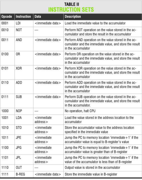
6. The LDI instruction loads the data in the accumulator specified
by the memory address of the RAM
7. The instruction register is cleared for next instruction
loading
CIRCUIT
Inputs to the accumulator, B-register, output register, PC register and memory address register are fed through the 8-bit parallel address/data bus. The input to the ALU is provided by the accumulator and B-register.
The ALU outputs to the bus via tristate buffers. The accumulator also outputs to the bus via tristate buffer 74LS245N. The tristate buffers are controlled by enable (G) pin.
The PC register output is fed to the program counter, providing the value to be loaded in the counter. The PC outputs to the bus via a tristate buffer. The memory address register outputs to the multiplexer.
The multiplexer output is fed to address pins of the RAM (CY6264). Input/output pins of the RAM are connected to the bus via the tristate buffer (IC23). The DIR and G pins of the tristate buffer are controlled based on the instruction and data flow. The 4-bit LSB of the bus is fed to the instruction register (74LS173N).
The inputs to the counter (CD4029N) are grounded. The outputs of the instruction register and the counter are connected to the address pins of ROMs (AT28C64). The ROM outputs are connected to enable pins of various ICs to control the data flow based on the state and instruction.
The functions of different modules in the architecture are
Program counter.
The program counter provides the computer with the current address of the instruction to be executed.
Memory address register.
The memory address register (MAR) stores the current address for the byte to be read or written from the memory.
Multiplexer.
The multiplexer allows selection of address either from the MAR (in run mode) or the manual input (programming mode).
Instruction register.
The instruction register of a computer stores the current instruction that is being executed.
During the computer’s operation, the value stored in instruction register is the instruction opcode. It forms the four bits of middle-value address (A4-A7) for ROMs. The counter for the next state provides the four bits of LSB (A0-A3) for ROMs. The 3-bit output from the comparator (74LS85N) forms the MSB (A8-A10). Thus, the address (A0-A10) is fed to the two ROMs to generate the control logic for different modules.
Output register.
It stores the value of the accumulator and displays the
result.
Clock. The clock pulse is generated by an NE555 timer chip
configured in astable mode.
ROM control
The two ROMs along with a 3-to-8 line decoder (74LS42N) provide a total of 18 control lines that control, enable or reset different parts of the computer. These control the clock enable pins of chips, thus controlling the data/instruction flow between various parts of the computer. The decoder output controls the tristates of the ALU controlling the data flow of the ALU result into the bus.
The ROM address is fed by the instruction register and counter. The data against the address for each state in the ROM is provided through the control lines or input/output pins.
Programming
Programming this computer is simple. There are two on/off switches (S8 for clock on/off and S7 for program/run mode selection), four pushbutton switches (S3 through S6) and two 8-bit DIP switches (one for address and the other for data). S3, S5 and S6 are reset switches, while S4 is RAM-write switch.
Toggle switch S7 to ‘program’ mode. The LED connected to it should turn off. Switch the clock to ‘off’ mode. Switch 8-bit address to the first address (0b00000001) and set the data DIP switch to the instruction/data to be written on the address. Press RAM-write switch S4 to load data onto the address. Similarly, repeat the process for successive code lines.
After entering all the codes/inputs, toggle program/run switch S7 to ‘run’ mode. Reset switches S3, S5 and S6 to clear all the LEDs. Press switch S8 on the clock to start computation. The maximum number of code lines that can be written for this project is 255.
Consider a hypothetical microprocessor generating a 16-bit address (for example, assume that the...
Consider a hypothetical microprocessor generating a 16-bit address (for example, assumethat the program counter and the address registers are 16 bits wide) and havinga 16-bit data bus.a. What is the maximum memory address space that the processor can access directlyif it is connected to a “16-bit memory”?b. What is the maximum memory address space that the processor can access directlyif it is connected to an “8-bit memory”?c. What architectural features will allow this microprocessor to access a separate“I/O space”?d. If...
3. (15 Pts.) In this problem you are given a microprocessor with 24-bit address bus and...
 3. (15 Pts.) In this problem you are given a microprocessor with 24-bit address bus and 8-bit data bus. a. What is the addressing space of this microprocessor? 113 16 MB b. how many bytes are contained in the sub-space starting at address C00 000h and ending at address DFF FFFH? Express your answer in KB and MB. DFFFEE CoO DOU - TFFFFF in ke 20 4SKe c. You would like to interface a single 4 MB memory IC to...
Exercise 1. What is the size of the memory for the microprocessor if it has 24-bit...
 Exercise 1. What is the size of the memory for the microprocessor if it has 24-bit address lines (bus)? Furthermore, give the starting address and the last address of the memory. 2. List the operation modes of the ARM Cortex-M3. 3. What is the function of register R13? Register R14? Register R15? 4. On an ARM Cortex-M3, in any given mode, how many registers does a programmer see at one time? 5. Which bits of the ARM Cortex-M3 status registers...
Design an 8-bit full adder using Verilog (Use only 1-bit full adders). Write the design code,...
Design an 8-bit full adder using Verilog (Use only 1-bit full adders). Write the design code, test-bench code of it, and test your design with six inputs. Note: Only use Verilog to design 8-bit full adder.
For my assignment, I've been asked to come up with a few questions to submit to...
For my assignment, I've been asked to come up with a few questions to submit to my classmates to answer in regards to Chapter 2 of Where the Girls Are: Growing up female with the Mass media. I have no idea where to begin. Can you give me some ideas? Thank you
Q4. 13 Marksl For 8085-based system, design a memory system using 8K 8-bit ROM +8-bit RAM...
 Q4. 13 Marksl For 8085-based system, design a memory system using 8K 8-bit ROM +8-bit RAM ICs to form 24K* 8-bit ROM and 24K 8-bit RAM. Use glue logic gates (NAND gates and Inverters) b) Use Decoder
Q4. 13 Marksl For 8085-based system, design a memory system using 8K 8-bit ROM +8-bit RAM ICs to form 24K* 8-bit ROM and 24K 8-bit RAM. Use glue logic gates (NAND gates and Inverters) b) Use Decoder
Q4. 13 Marksl For 8085-based system, design a memory system using 8K 8-bit ROM +8-bit RAM ICs to form 24K* 8-bit ROM and 24K 8-bit RAM. Use glue logic gates (NAND gates and Inverters) b) Use Decoder
Computer Architecture 2) (10 points) Consider a microprocessor driven by an 8-MHz input clock, with a...
 Computer Architecture
2) (10 points) Consider a microprocessor driven by an 8-MHz input clock, with a 16-bit external data bus. Assume that this microprocessor has a bus cycle whose minimum duration equals 4 input clock cycles. A bus cycle is the number of clock cycles required to accomplish a task (such as data transfer). What is the maximum data transfer rate across the bus that this microprocessor can sustain, in bytes?
Computer Architecture
2) (10 points) Consider a microprocessor driven by an 8-MHz input clock, with a 16-bit external data bus. Assume that this microprocessor has a bus cycle whose minimum duration equals 4 input clock cycles. A bus cycle is the number of clock cycles required to accomplish a task (such as data transfer). What is the maximum data transfer rate across the bus that this microprocessor can sustain, in bytes?
1. Cache memory (8pts) Consider adding cache to a processor-memory system design. The microprocessor without cache needs 12 clock cycles to read a 16-bit word from the memory. With cache, it take...
 1. Cache memory (8pts) Consider adding cache to a processor-memory system design. The microprocessor without cache needs 12 clock cycles to read a 16-bit word from the memory. With cache, it takes only 4 clock cycles if the data happens to be in the cache and a total 20 clock cycles including the cache misses. a. What is the performance ratio of the cache system to the non-cache system given a hit rate of 80%? b. For what hit rate...
Design a combinational circuit design that given a four-bit number as the input outputs an 8-bit...
Design a combinational circuit design that given a four-bit number as the input outputs an 8-bit number that represents the nth Fibonacci number in the sequence. For instance, if the input is 0001, the output should be the second number in the Fibonacci sequence. The Fibonacci series looks like the following: 0, 1, 1, 2, 3, 5, 8, 13, and so on. The first two numbers in the sequence are always 0 and 1. However, after that, you must add...
Design 5 seconds. Use 8-bit counter and logic gates for your hardware design Assume clock frequency...
 Design 5 seconds. Use 8-bit counter and logic gates for your hardware design Assume clock frequency of 80 Hz for the 8-bit counters that are used in the design Show all work and provide the logic diagram for full credit Watchdog-Timer that will generate an overflow (interrupt) output every a
Design 5 seconds. Use 8-bit counter and logic gates for your hardware design Assume clock frequency of 80 Hz for the 8-bit counters that are used in the design Show...
Design 5 seconds. Use 8-bit counter and logic gates for your hardware design Assume clock frequency of 80 Hz for the 8-bit counters that are used in the design Show all work and provide the logic diagram for full credit Watchdog-Timer that will generate an overflow (interrupt) output every a
Design 5 seconds. Use 8-bit counter and logic gates for your hardware design Assume clock frequency of 80 Hz for the 8-bit counters that are used in the design Show...
 3. (15 Pts.) In this problem you are given a microprocessor with 24-bit address bus and 8-bit data bus. a. What is the addressing space of this microprocessor? 113 16 MB b. how many bytes are contained in the sub-space starting at address C00 000h and ending at address DFF FFFH? Express your answer in KB and MB. DFFFEE CoO DOU - TFFFFF in ke 20 4SKe c. You would like to interface a single 4 MB memory IC to...
 Exercise 1. What is the size of the memory for the microprocessor if it has 24-bit address lines (bus)? Furthermore, give the starting address and the last address of the memory. 2. List the operation modes of the ARM Cortex-M3. 3. What is the function of register R13? Register R14? Register R15? 4. On an ARM Cortex-M3, in any given mode, how many registers does a programmer see at one time? 5. Which bits of the ARM Cortex-M3 status registers...
 Q4. 13 Marksl For 8085-based system, design a memory system using 8K 8-bit ROM +8-bit RAM ICs to form 24K* 8-bit ROM and 24K 8-bit RAM. Use glue logic gates (NAND gates and Inverters) b) Use Decoder
Q4. 13 Marksl For 8085-based system, design a memory system using 8K 8-bit ROM +8-bit RAM ICs to form 24K* 8-bit ROM and 24K 8-bit RAM. Use glue logic gates (NAND gates and Inverters) b) Use Decoder
Q4. 13 Marksl For 8085-based system, design a memory system using 8K 8-bit ROM +8-bit RAM ICs to form 24K* 8-bit ROM and 24K 8-bit RAM. Use glue logic gates (NAND gates and Inverters) b) Use Decoder
 Computer Architecture
2) (10 points) Consider a microprocessor driven by an 8-MHz input clock, with a 16-bit external data bus. Assume that this microprocessor has a bus cycle whose minimum duration equals 4 input clock cycles. A bus cycle is the number of clock cycles required to accomplish a task (such as data transfer). What is the maximum data transfer rate across the bus that this microprocessor can sustain, in bytes?
Computer Architecture
2) (10 points) Consider a microprocessor driven by an 8-MHz input clock, with a 16-bit external data bus. Assume that this microprocessor has a bus cycle whose minimum duration equals 4 input clock cycles. A bus cycle is the number of clock cycles required to accomplish a task (such as data transfer). What is the maximum data transfer rate across the bus that this microprocessor can sustain, in bytes?
 1. Cache memory (8pts) Consider adding cache to a processor-memory system design. The microprocessor without cache needs 12 clock cycles to read a 16-bit word from the memory. With cache, it takes only 4 clock cycles if the data happens to be in the cache and a total 20 clock cycles including the cache misses. a. What is the performance ratio of the cache system to the non-cache system given a hit rate of 80%? b. For what hit rate...
 Design 5 seconds. Use 8-bit counter and logic gates for your hardware design Assume clock frequency of 80 Hz for the 8-bit counters that are used in the design Show all work and provide the logic diagram for full credit Watchdog-Timer that will generate an overflow (interrupt) output every a
Design 5 seconds. Use 8-bit counter and logic gates for your hardware design Assume clock frequency of 80 Hz for the 8-bit counters that are used in the design Show...
Design 5 seconds. Use 8-bit counter and logic gates for your hardware design Assume clock frequency of 80 Hz for the 8-bit counters that are used in the design Show all work and provide the logic diagram for full credit Watchdog-Timer that will generate an overflow (interrupt) output every a
Design 5 seconds. Use 8-bit counter and logic gates for your hardware design Assume clock frequency of 80 Hz for the 8-bit counters that are used in the design Show...
Most questions answered within 3 hours.
-
Assume that the population of Mexico is 128
million and that the population increases 1.01
percentannually....
asked 49 minutes ago -
Can someone please help me add appropriate descriptive
comments to each line of code in the...
asked 55 minutes ago -
Romeo wishes to throw a bouquet of flowers to Juliet, who is on
a second-story balcony,...
asked 1 hour ago -
Why is QE a controversial monetary policy tool.
A. It may lead to excessive inflation.B. By...
asked 2 hours ago -
Principles of Programming midterm study guide help!
1.)
______ Which of the following would reference the...
asked 1 hour ago -
A finite potential well has depth U0 = 2.78 eV . What is the
penetration distance...
asked 2 hours ago -
1. The bus bars of a power station are in two sections A and B
separated...
asked 2 hours ago -
Fiscal policy is the deliberate manipulation of taxes and
government spending to alter GDP, employment, inflation...
asked 3 hours ago -
evaluating an expression using only one digit and + and - as
operators ....3+5-1+7-5+8
-----------------------
stack...
asked 3 hours ago -
Two concentric current loops lie in the same plane. The smaller
loop has a radius of...
asked 3 hours ago -
1)Which of the following is an
important difference between qualified and nonqualified retirement
plans?
a. Qualified...
asked 4 hours ago -
What's the streaming business's problem on the
horizon?
asked 5 hours ago