
Homework Answers


Add Answer to:
Design an ideal abrupt silicon PN-junction at 300 K such that the donor impurity concentration in...
this is a problem of semiconductor device and fundamentals. Problem 4: pn Junction Current Distributions Consider a...
 this is a problem of semiconductor device and
fundamentals.
Problem 4: pn Junction Current Distributions Consider a Si pn step junction diode maintained at room temperature, with p-side and n-side dopant concentrations NA 1016 cm3 and Np-2x1016 cm3, respectively. (You may assume that each side is uncompensated.) The minority carrier recombination lifetimes are τ,-10-6 s and τ,-10-7 s on the p-side and n-side, respectively a) Calculate the minority carrier densities at the edges of the depletion region when the applied...
this is a problem of semiconductor device and
fundamentals.
Problem 4: pn Junction Current Distributions Consider a Si pn step junction diode maintained at room temperature, with p-side and n-side dopant concentrations NA 1016 cm3 and Np-2x1016 cm3, respectively. (You may assume that each side is uncompensated.) The minority carrier recombination lifetimes are τ,-10-6 s and τ,-10-7 s on the p-side and n-side, respectively a) Calculate the minority carrier densities at the edges of the depletion region when the applied...
A silicon pn junction at T = 300 K has the following parameters: Na-5 1016 cm-?,...
 A silicon pn junction at T = 300 K has the following parameters: Na-5 1016 cm-?, N,-1 1016 cm-3, D.-25 cm3/s, D.-10 cm2/s, ?,0-5 x 10⁻⁷ s, and To 1 X 10⁻⁷ s. The cross-sectional area is A 10-3 cm2 and the forward- bias voltage is V,-0.625 V. Calculate the (a) minority electron diffusion cur- rent at the space charge edge, (b) minority hole diffusion current at the space charge edge, and (c) total current in the pn junction diode.
Problem 4: An abrupt silicon p-n junction diode has the following characteristics. side n-side N-4x 1016cm N1016cm3 n 1000 cm2/V sec 350 cm2/V sec Area A 102cm2 Calculate the following quantities...
 Problem 4: An abrupt silicon p-n junction diode has the following characteristics. side n-side N-4x 1016cm N1016cm3 n 1000 cm2/V sec 350 cm2/V sec Area A 102cm2 Calculate the following quantities: (a) Reverse saturation hole current component (b) Reverse saturation electron current component. (c) Minority carrier concentrations at the edge of the depletion layer, p(0) and pr(0), for a forward voltage of 0.6 V (d) Electron and hole current for the bias condition of (c). (e) Make a rough sketch...
Problem 4 (25 points) Consider a silicon pn junction at T-300 K, NA-ND- 1x101° cm3. The minority ...
 Problem 4 (25 points) Consider a silicon pn junction at T-300 K, NA-ND- 1x101° cm3. The minority carrier lifetimes are τ n-0.01 μs and τ p-0.01 us. The junction is forwardbiased with Va 0.6V. The minority carrier diffusion coefficients are Dn-20 cm s, Dp 10 cm Is. n.-1.5x 1010 cm-3 Depletion region n-type p-type a) (10 points) Calculate the excess electron concentration as a function of x in the p side (see the figure above). b) (5 points) Calculate the...
Problem 3 (25 points) Consider a silicon pn junction at T - 300 K, NA- 1016 cm3, ND-5x1016 cm-3. The minority carrier lifetimes are τα , τ,-1 us. The junction is forward biased with Va-0.5V The minor...
 Problem 3 (25 points) Consider a silicon pn junction at T - 300 K, NA- 1016 cm3, ND-5x1016 cm-3. The minority carrier lifetimes are τα , τ,-1 us. The junction is forward biased with Va-0.5V The minority carrier diffusion coefficients are D 25 cm/s, Da- 10 cm2/s n,1.5x1010 cm3 kT 0.0267 Depletion region p-type n-type a) (5 points) Calculate the excess electron concentration as a function of x in the p-side (see the figure above) b) (10 points) Calculate the...
Problem 4 (25 points) Consider a silicon pn junction at T-300 K, NA-ND- 1x101° cm3. The minority ...
 Can someone help solve this question step by step? Thanks!
Problem 4 (25 points) Consider a silicon pn junction at T-300 K, NA-ND- 1x101° cm3. The minority carrier lifetimes are τ n-0.01 μs and τ p-0.01 us. The junction is forwardbiased with Va 0.6V. The minority carrier diffusion coefficients are Dn-20 cm s, Dp 10 cm Is. n.-1.5x 1010 cm-3 Depletion region n-type p-type a) (10 points) Calculate the excess electron concentration as a function of x in the p...
Can someone help solve this question step by step? Thanks!
Problem 4 (25 points) Consider a silicon pn junction at T-300 K, NA-ND- 1x101° cm3. The minority carrier lifetimes are τ n-0.01 μs and τ p-0.01 us. The junction is forwardbiased with Va 0.6V. The minority carrier diffusion coefficients are Dn-20 cm s, Dp 10 cm Is. n.-1.5x 1010 cm-3 Depletion region n-type p-type a) (10 points) Calculate the excess electron concentration as a function of x in the p...
Problem 4 (25 points) Consider a silicon pn junction at T 300 K, NA ND-1x1016 cm3....
 Problem 4 (25 points) Consider a silicon pn junction at T 300 K, NA ND-1x1016 cm3. The minority carrier lifetimes are τ -0.01 μs and τΡ 0.01 μ. The Junction is forwardbiased with , V,-0.6V. The minority carrier diffusion coefficients are D,-20 cm2/s, D,-10 cm2/s. n, = 1.5x 1010cm -3 Depletion region n-type p-type a) (10 points) Calculate the excess electron concentration as a function of x in the p side (see the figure above). b) (5 points) Calculate the...
Consider a silicon pn junction at T = 300 K, NA-Np - 4x106cm. The minority carrier...
 Consider a silicon pn junction at T = 300 K, NA-Np - 4x106cm. The minority carrier lifetimes are tn = Tp=1 us. The junction is forward biased with V, -0.6V. The minority carrier diffusion coefficients are D = 20 cm²/s, D = 10 cm²/s. n;= 1.5x100cm, kt/e = 0.026V Depletion region n-type p-type a) (5 points) Do we have low-level injection? b) (10 points) Calculate the electron concentration at x = -(Xp + Ln) where L, is the electron diffusion...
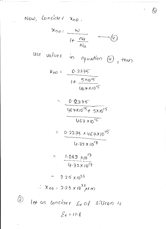
Consider a silicon pn step junction diode with NA-1x1018 cm3 and No 1x1017cm-3, maintained at T...
 Consider a silicon pn step junction diode with NA-1x1018 cm3 and No 1x1017cm-3, maintained at T 300K. The minority carrier lifetimes in the p-side and n-side are τη-10-8 s and Tp-10-7 s, respectively. a) Calculate the minority carrier densities at the edges of the depletion region when the applied voltage (VA) is 0.6 V. of the junction, for the applied bias voltage of part (a) densities are equal in magnitude, for the applied voltage of part (a). b) Sketch the...
3.13 Si pn junction Consider a long pn junction diode with an acceptor doping Naof 1018 cm-3 on t...
 3.13 Si pn junction Consider a long pn junction diode with an acceptor doping Naof 1018 cm-3 on the p-side and donor concentration of Nj on the n-side. The diode is forward biased and has a voltage of 0.6 V across it. The diode cross-sectional area is 1 mm2. The minority carrier recombination time, T, depends on the total dopant concentration, Ndopant (cm), through the following approximate empirical relation (5x 10⁻⁷)/(1 + 2 10-17N1°pan.) where T is in seconds. (a)...
 this is a problem of semiconductor device and
fundamentals.
Problem 4: pn Junction Current Distributions Consider a Si pn step junction diode maintained at room temperature, with p-side and n-side dopant concentrations NA 1016 cm3 and Np-2x1016 cm3, respectively. (You may assume that each side is uncompensated.) The minority carrier recombination lifetimes are τ,-10-6 s and τ,-10-7 s on the p-side and n-side, respectively a) Calculate the minority carrier densities at the edges of the depletion region when the applied...
this is a problem of semiconductor device and
fundamentals.
Problem 4: pn Junction Current Distributions Consider a Si pn step junction diode maintained at room temperature, with p-side and n-side dopant concentrations NA 1016 cm3 and Np-2x1016 cm3, respectively. (You may assume that each side is uncompensated.) The minority carrier recombination lifetimes are τ,-10-6 s and τ,-10-7 s on the p-side and n-side, respectively a) Calculate the minority carrier densities at the edges of the depletion region when the applied...
 A silicon pn junction at T = 300 K has the following parameters: Na-5 1016 cm-?, N,-1 1016 cm-3, D.-25 cm3/s, D.-10 cm2/s, ?,0-5 x 10⁻⁷ s, and To 1 X 10⁻⁷ s. The cross-sectional area is A 10-3 cm2 and the forward- bias voltage is V,-0.625 V. Calculate the (a) minority electron diffusion cur- rent at the space charge edge, (b) minority hole diffusion current at the space charge edge, and (c) total current in the pn junction diode.
 Problem 4: An abrupt silicon p-n junction diode has the following characteristics. side n-side N-4x 1016cm N1016cm3 n 1000 cm2/V sec 350 cm2/V sec Area A 102cm2 Calculate the following quantities: (a) Reverse saturation hole current component (b) Reverse saturation electron current component. (c) Minority carrier concentrations at the edge of the depletion layer, p(0) and pr(0), for a forward voltage of 0.6 V (d) Electron and hole current for the bias condition of (c). (e) Make a rough sketch...
 Problem 4 (25 points) Consider a silicon pn junction at T-300 K, NA-ND- 1x101° cm3. The minority carrier lifetimes are τ n-0.01 μs and τ p-0.01 us. The junction is forwardbiased with Va 0.6V. The minority carrier diffusion coefficients are Dn-20 cm s, Dp 10 cm Is. n.-1.5x 1010 cm-3 Depletion region n-type p-type a) (10 points) Calculate the excess electron concentration as a function of x in the p side (see the figure above). b) (5 points) Calculate the...
 Problem 3 (25 points) Consider a silicon pn junction at T - 300 K, NA- 1016 cm3, ND-5x1016 cm-3. The minority carrier lifetimes are τα , τ,-1 us. The junction is forward biased with Va-0.5V The minority carrier diffusion coefficients are D 25 cm/s, Da- 10 cm2/s n,1.5x1010 cm3 kT 0.0267 Depletion region p-type n-type a) (5 points) Calculate the excess electron concentration as a function of x in the p-side (see the figure above) b) (10 points) Calculate the...
 Can someone help solve this question step by step? Thanks!
Problem 4 (25 points) Consider a silicon pn junction at T-300 K, NA-ND- 1x101° cm3. The minority carrier lifetimes are τ n-0.01 μs and τ p-0.01 us. The junction is forwardbiased with Va 0.6V. The minority carrier diffusion coefficients are Dn-20 cm s, Dp 10 cm Is. n.-1.5x 1010 cm-3 Depletion region n-type p-type a) (10 points) Calculate the excess electron concentration as a function of x in the p...
Can someone help solve this question step by step? Thanks!
Problem 4 (25 points) Consider a silicon pn junction at T-300 K, NA-ND- 1x101° cm3. The minority carrier lifetimes are τ n-0.01 μs and τ p-0.01 us. The junction is forwardbiased with Va 0.6V. The minority carrier diffusion coefficients are Dn-20 cm s, Dp 10 cm Is. n.-1.5x 1010 cm-3 Depletion region n-type p-type a) (10 points) Calculate the excess electron concentration as a function of x in the p...
 Problem 4 (25 points) Consider a silicon pn junction at T 300 K, NA ND-1x1016 cm3. The minority carrier lifetimes are τ -0.01 μs and τΡ 0.01 μ. The Junction is forwardbiased with , V,-0.6V. The minority carrier diffusion coefficients are D,-20 cm2/s, D,-10 cm2/s. n, = 1.5x 1010cm -3 Depletion region n-type p-type a) (10 points) Calculate the excess electron concentration as a function of x in the p side (see the figure above). b) (5 points) Calculate the...
 Consider a silicon pn junction at T = 300 K, NA-Np - 4x106cm. The minority carrier lifetimes are tn = Tp=1 us. The junction is forward biased with V, -0.6V. The minority carrier diffusion coefficients are D = 20 cm²/s, D = 10 cm²/s. n;= 1.5x100cm, kt/e = 0.026V Depletion region n-type p-type a) (5 points) Do we have low-level injection? b) (10 points) Calculate the electron concentration at x = -(Xp + Ln) where L, is the electron diffusion...
 Consider a silicon pn step junction diode with NA-1x1018 cm3 and No 1x1017cm-3, maintained at T 300K. The minority carrier lifetimes in the p-side and n-side are τη-10-8 s and Tp-10-7 s, respectively. a) Calculate the minority carrier densities at the edges of the depletion region when the applied voltage (VA) is 0.6 V. of the junction, for the applied bias voltage of part (a) densities are equal in magnitude, for the applied voltage of part (a). b) Sketch the...
 3.13 Si pn junction Consider a long pn junction diode with an acceptor doping Naof 1018 cm-3 on the p-side and donor concentration of Nj on the n-side. The diode is forward biased and has a voltage of 0.6 V across it. The diode cross-sectional area is 1 mm2. The minority carrier recombination time, T, depends on the total dopant concentration, Ndopant (cm), through the following approximate empirical relation (5x 10⁻⁷)/(1 + 2 10-17N1°pan.) where T is in seconds. (a)...
Most questions answered within 3 hours.
-
Accent Software faces the following conditions. All of these
support Accent’s use of a market-penetration pricing...
asked 36 minutes ago -
A mathematically inclined friend emails you the following
instructions: "Meet me in the cafeteria the first...
asked 38 minutes ago -
A monopoly sells in two countries . The demand curves in the two
countries are p1...
asked 1 hour ago -
A .15kg rubber ball is bounced off a wall. Before hitting the
wall, the ball moves...
asked 2 hours ago -
A manufacturing company preparing to build a new plant is
considering three potential locations for it....
asked 2 hours ago -
B. If compound Y has approximately the same values of solubility
in toluene as compound X,...
asked 3 hours ago -
Oscar Inc. has inventory in Japan valued at 39,051,000 Yen one
year ago. One year ago...
asked 3 hours ago -
If Canada suffered from "fundamental disequilibrium," and its
government choose not to devalue its currency, a...
asked 3 hours ago -
4. How many input & output Key Value Pairs are passed into,
and emitted out of...
asked 3 hours ago -
Why would your heart not function well if constructed of
skeletal muscle? What is the particular...
asked 3 hours ago -
Please respond to this essay question in full essay form for
Chemistry 1102 Organic and Biochemistry:...
asked 3 hours ago -
Determine the head loss and velocity of flow in a water supply main
of 15.0 cm...
asked 3 hours ago