
Homework Answers

Add Answer to:
Problem 3 (25 points) Consider a silicon pn junction at T - 300 K, NA- 1016 cm3, ND-5x1016 cm-3. The minority carrier lifetimes are τα , τ,-1 us. The junction is forward biased with Va-0.5V The minor...
Problem 4 (25 points) Consider a silicon pn junction at T-300 K, NA-ND- 1x101° cm3. The minority ...
 Problem 4 (25 points) Consider a silicon pn junction at T-300 K, NA-ND- 1x101° cm3. The minority carrier lifetimes are τ n-0.01 μs and τ p-0.01 us. The junction is forwardbiased with Va 0.6V. The minority carrier diffusion coefficients are Dn-20 cm s, Dp 10 cm Is. n.-1.5x 1010 cm-3 Depletion region n-type p-type a) (10 points) Calculate the excess electron concentration as a function of x in the p side (see the figure above). b) (5 points) Calculate the...
Problem 4 (25 points) Consider a silicon pn junction at T-300 K, NA-ND- 1x101° cm3. The minority ...
 Can someone help solve this question step by step? Thanks!
Problem 4 (25 points) Consider a silicon pn junction at T-300 K, NA-ND- 1x101° cm3. The minority carrier lifetimes are τ n-0.01 μs and τ p-0.01 us. The junction is forwardbiased with Va 0.6V. The minority carrier diffusion coefficients are Dn-20 cm s, Dp 10 cm Is. n.-1.5x 1010 cm-3 Depletion region n-type p-type a) (10 points) Calculate the excess electron concentration as a function of x in the p...
Can someone help solve this question step by step? Thanks!
Problem 4 (25 points) Consider a silicon pn junction at T-300 K, NA-ND- 1x101° cm3. The minority carrier lifetimes are τ n-0.01 μs and τ p-0.01 us. The junction is forwardbiased with Va 0.6V. The minority carrier diffusion coefficients are Dn-20 cm s, Dp 10 cm Is. n.-1.5x 1010 cm-3 Depletion region n-type p-type a) (10 points) Calculate the excess electron concentration as a function of x in the p...
Consider a silicon pn junction at T = 300 K, NA-Np - 4x106cm. The minority carrier...
 Consider a silicon pn junction at T = 300 K, NA-Np - 4x106cm. The minority carrier lifetimes are tn = Tp=1 us. The junction is forward biased with V, -0.6V. The minority carrier diffusion coefficients are D = 20 cm²/s, D = 10 cm²/s. n;= 1.5x100cm, kt/e = 0.026V Depletion region n-type p-type a) (5 points) Do we have low-level injection? b) (10 points) Calculate the electron concentration at x = -(Xp + Ln) where L, is the electron diffusion...
Problem 4 (25 points) Consider a silicon pn junction at T 300 K, NA ND-1x1016 cm3....
 Problem 4 (25 points) Consider a silicon pn junction at T 300 K, NA ND-1x1016 cm3. The minority carrier lifetimes are τ -0.01 μs and τΡ 0.01 μ. The Junction is forwardbiased with , V,-0.6V. The minority carrier diffusion coefficients are D,-20 cm2/s, D,-10 cm2/s. n, = 1.5x 1010cm -3 Depletion region n-type p-type a) (10 points) Calculate the excess electron concentration as a function of x in the p side (see the figure above). b) (5 points) Calculate the...
Problem 4 (25 points) Consider a silicon pn junction at T-300 K, N,-1x10¹⁷ ст?, ND-11016 Cm -, The minority carrier lifetimes are τ u-^ 1 μs and τ p-1 μs. The minority carrier diffusion coefficients...
 Problem 4 (25 points) Consider a silicon pn junction at T-300 K, N,-1x10¹⁷ ст?, ND-11016 Cm -, The minority carrier lifetimes are τ u-^ 1 μs and τ p-1 μs. The minority carrier diffusion coefficients are Da-25 cm2/s, DR-10 cm2/s. n1-1.5x1010 cm -3 kT - 0.026V Low-level injection is defined to be when the minority carrier concentration at the edge of the space charge region becomes equal to one-tenth the majority carrier concentration. Determine the value of the voltage across...
Problem 7: A silicon diode is asymmetrically doped at ND-10', cm? and N-1016 cm'. (Note that...
 Problem 7: A silicon diode is asymmetrically doped at ND-10', cm? and N-1016 cm'. (Note that at N 10" the semiconductor is on the edge of degeneracy, but we can assume that non-degenerate carrier statistics are close enough for this problem.) Answer the following questions assuming room temperature. Assume that the minority electron and hole lifetimes are τ.-, 10's. The lengths of the N and P regions are L = 500 μm and 1. >> x,,x . a) Find the...
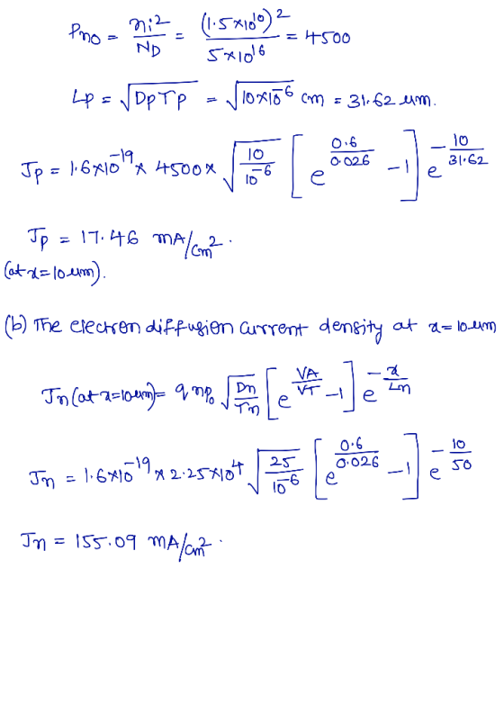
A silicon pn junction at T = 300 K has the following parameters: Na-5 1016 cm-?,...
 A silicon pn junction at T = 300 K has the following parameters: Na-5 1016 cm-?, N,-1 1016 cm-3, D.-25 cm3/s, D.-10 cm2/s, ?,0-5 x 10⁻⁷ s, and To 1 X 10⁻⁷ s. The cross-sectional area is A 10-3 cm2 and the forward- bias voltage is V,-0.625 V. Calculate the (a) minority electron diffusion cur- rent at the space charge edge, (b) minority hole diffusion current at the space charge edge, and (c) total current in the pn junction diode.
this is a problem of semiconductor device and fundamentals. Problem 4: pn Junction Current Distributions Consider a...
 this is a problem of semiconductor device and
fundamentals.
Problem 4: pn Junction Current Distributions Consider a Si pn step junction diode maintained at room temperature, with p-side and n-side dopant concentrations NA 1016 cm3 and Np-2x1016 cm3, respectively. (You may assume that each side is uncompensated.) The minority carrier recombination lifetimes are τ,-10-6 s and τ,-10-7 s on the p-side and n-side, respectively a) Calculate the minority carrier densities at the edges of the depletion region when the applied...
this is a problem of semiconductor device and
fundamentals.
Problem 4: pn Junction Current Distributions Consider a Si pn step junction diode maintained at room temperature, with p-side and n-side dopant concentrations NA 1016 cm3 and Np-2x1016 cm3, respectively. (You may assume that each side is uncompensated.) The minority carrier recombination lifetimes are τ,-10-6 s and τ,-10-7 s on the p-side and n-side, respectively a) Calculate the minority carrier densities at the edges of the depletion region when the applied...
Consider a silicon pn step junction diode with NA-1x1018 cm3 and No 1x1017cm-3, maintained at T...
 Consider a silicon pn step junction diode with NA-1x1018 cm3 and No 1x1017cm-3, maintained at T 300K. The minority carrier lifetimes in the p-side and n-side are τη-10-8 s and Tp-10-7 s, respectively. a) Calculate the minority carrier densities at the edges of the depletion region when the applied voltage (VA) is 0.6 V. of the junction, for the applied bias voltage of part (a) densities are equal in magnitude, for the applied voltage of part (a). b) Sketch the...
3. A silicon step junction has uniform impurity doping concentrations of N. 5 x 1015 cm-3 and Nd ...
 3. A silicon step junction has uniform impurity doping concentrations of N. 5 x 1015 cm-3 and Nd = 1 x 1015 cm-, and a cross-sectional area of A-|0-4 cm2. Let tao -0.4 s and tpo 0.1 us. Consider the geometry in Figure.Calculate (a) the ideal reverse saturation current due to holes, (b) the ideal reverse saturation current due to electrons, (c) the hole concentration at a, if V V and (d) the electron current at x = x" +...
 Problem 4 (25 points) Consider a silicon pn junction at T-300 K, NA-ND- 1x101° cm3. The minority carrier lifetimes are τ n-0.01 μs and τ p-0.01 us. The junction is forwardbiased with Va 0.6V. The minority carrier diffusion coefficients are Dn-20 cm s, Dp 10 cm Is. n.-1.5x 1010 cm-3 Depletion region n-type p-type a) (10 points) Calculate the excess electron concentration as a function of x in the p side (see the figure above). b) (5 points) Calculate the...
 Can someone help solve this question step by step? Thanks!
Problem 4 (25 points) Consider a silicon pn junction at T-300 K, NA-ND- 1x101° cm3. The minority carrier lifetimes are τ n-0.01 μs and τ p-0.01 us. The junction is forwardbiased with Va 0.6V. The minority carrier diffusion coefficients are Dn-20 cm s, Dp 10 cm Is. n.-1.5x 1010 cm-3 Depletion region n-type p-type a) (10 points) Calculate the excess electron concentration as a function of x in the p...
Can someone help solve this question step by step? Thanks!
Problem 4 (25 points) Consider a silicon pn junction at T-300 K, NA-ND- 1x101° cm3. The minority carrier lifetimes are τ n-0.01 μs and τ p-0.01 us. The junction is forwardbiased with Va 0.6V. The minority carrier diffusion coefficients are Dn-20 cm s, Dp 10 cm Is. n.-1.5x 1010 cm-3 Depletion region n-type p-type a) (10 points) Calculate the excess electron concentration as a function of x in the p...
 Consider a silicon pn junction at T = 300 K, NA-Np - 4x106cm. The minority carrier lifetimes are tn = Tp=1 us. The junction is forward biased with V, -0.6V. The minority carrier diffusion coefficients are D = 20 cm²/s, D = 10 cm²/s. n;= 1.5x100cm, kt/e = 0.026V Depletion region n-type p-type a) (5 points) Do we have low-level injection? b) (10 points) Calculate the electron concentration at x = -(Xp + Ln) where L, is the electron diffusion...
 Problem 4 (25 points) Consider a silicon pn junction at T 300 K, NA ND-1x1016 cm3. The minority carrier lifetimes are τ -0.01 μs and τΡ 0.01 μ. The Junction is forwardbiased with , V,-0.6V. The minority carrier diffusion coefficients are D,-20 cm2/s, D,-10 cm2/s. n, = 1.5x 1010cm -3 Depletion region n-type p-type a) (10 points) Calculate the excess electron concentration as a function of x in the p side (see the figure above). b) (5 points) Calculate the...
 Problem 4 (25 points) Consider a silicon pn junction at T-300 K, N,-1x10¹⁷ ст?, ND-11016 Cm -, The minority carrier lifetimes are τ u-^ 1 μs and τ p-1 μs. The minority carrier diffusion coefficients are Da-25 cm2/s, DR-10 cm2/s. n1-1.5x1010 cm -3 kT - 0.026V Low-level injection is defined to be when the minority carrier concentration at the edge of the space charge region becomes equal to one-tenth the majority carrier concentration. Determine the value of the voltage across...
 Problem 7: A silicon diode is asymmetrically doped at ND-10', cm? and N-1016 cm'. (Note that at N 10" the semiconductor is on the edge of degeneracy, but we can assume that non-degenerate carrier statistics are close enough for this problem.) Answer the following questions assuming room temperature. Assume that the minority electron and hole lifetimes are τ.-, 10's. The lengths of the N and P regions are L = 500 μm and 1. >> x,,x . a) Find the...
 A silicon pn junction at T = 300 K has the following parameters: Na-5 1016 cm-?, N,-1 1016 cm-3, D.-25 cm3/s, D.-10 cm2/s, ?,0-5 x 10⁻⁷ s, and To 1 X 10⁻⁷ s. The cross-sectional area is A 10-3 cm2 and the forward- bias voltage is V,-0.625 V. Calculate the (a) minority electron diffusion cur- rent at the space charge edge, (b) minority hole diffusion current at the space charge edge, and (c) total current in the pn junction diode.
 this is a problem of semiconductor device and
fundamentals.
Problem 4: pn Junction Current Distributions Consider a Si pn step junction diode maintained at room temperature, with p-side and n-side dopant concentrations NA 1016 cm3 and Np-2x1016 cm3, respectively. (You may assume that each side is uncompensated.) The minority carrier recombination lifetimes are τ,-10-6 s and τ,-10-7 s on the p-side and n-side, respectively a) Calculate the minority carrier densities at the edges of the depletion region when the applied...
this is a problem of semiconductor device and
fundamentals.
Problem 4: pn Junction Current Distributions Consider a Si pn step junction diode maintained at room temperature, with p-side and n-side dopant concentrations NA 1016 cm3 and Np-2x1016 cm3, respectively. (You may assume that each side is uncompensated.) The minority carrier recombination lifetimes are τ,-10-6 s and τ,-10-7 s on the p-side and n-side, respectively a) Calculate the minority carrier densities at the edges of the depletion region when the applied...
 Consider a silicon pn step junction diode with NA-1x1018 cm3 and No 1x1017cm-3, maintained at T 300K. The minority carrier lifetimes in the p-side and n-side are τη-10-8 s and Tp-10-7 s, respectively. a) Calculate the minority carrier densities at the edges of the depletion region when the applied voltage (VA) is 0.6 V. of the junction, for the applied bias voltage of part (a) densities are equal in magnitude, for the applied voltage of part (a). b) Sketch the...
 3. A silicon step junction has uniform impurity doping concentrations of N. 5 x 1015 cm-3 and Nd = 1 x 1015 cm-, and a cross-sectional area of A-|0-4 cm2. Let tao -0.4 s and tpo 0.1 us. Consider the geometry in Figure.Calculate (a) the ideal reverse saturation current due to holes, (b) the ideal reverse saturation current due to electrons, (c) the hole concentration at a, if V V and (d) the electron current at x = x" +...
Most questions answered within 3 hours.
-
Suppose N packets are sent,
and each packet arrives at rate of L/2R to a link....
asked 3 minutes ago -
17. Show the steps involved in reduction of the ketone in fatty
acid synthesis. Which cofactor...
asked 4 minutes ago -
5.61 g of octane, C8H18, reacts with excess oxygen in a bomb
calorimeter. The heat capacity...
asked 8 minutes ago -
The velocity field of a flow is given by V = (2+1) x
y2 i +...
asked 17 minutes ago -
(EPS with
Convertible Bonds) On June 1, 2012, Bluhm Company and
Amanar Company merged to form...
asked 15 minutes ago -
2. Discuss why the study exemplifies one that agrees with The
American Psychological Association’s (APA) Ethical...
asked 19 minutes ago -
Without considering the following capital gains and losses,
Charlene, who is single, has a taxable income...
asked 26 minutes ago -
1a. The __________ functional group often triggers our sense of
smell.
1b. The geometry around a...
asked 39 minutes ago -
A uniform plank of length 2.00 m and mass 34.0 kg is supported
by three ropes,...
asked 40 minutes ago -
Suppose a floor on a hospital has 12 physicians at any given
time. You are brought...
asked 54 minutes ago -
Compartmentalization
in eukaryotic cells facilitates chemical reactions happening faster
due to... Select all
Substrates needed for...
asked 41 minutes ago -
The deltaH for the solution process when solid sodium
hydroxide dissolves in water is 44.4 kJ/mol....
asked 44 minutes ago