
Homework Answers
Add Answer to:
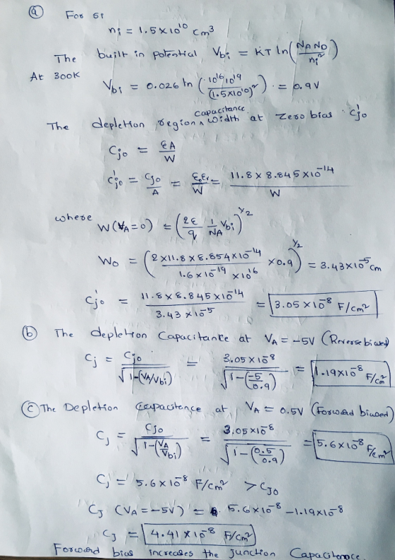
Problem 7: A silicon diode is asymmetrically doped at ND-10', cm? and N-1016 cm'. (Note that...
Problem 3 (25 points) Consider a silicon pn junction at T - 300 K, NA- 1016 cm3, ND-5x1016 cm-3. The minority carrier lifetimes are τα , τ,-1 us. The junction is forward biased with Va-0.5V The minor...
 Problem 3 (25 points) Consider a silicon pn junction at T - 300 K, NA- 1016 cm3, ND-5x1016 cm-3. The minority carrier lifetimes are τα , τ,-1 us. The junction is forward biased with Va-0.5V The minority carrier diffusion coefficients are D 25 cm/s, Da- 10 cm2/s n,1.5x1010 cm3 kT 0.0267 Depletion region p-type n-type a) (5 points) Calculate the excess electron concentration as a function of x in the p-side (see the figure above) b) (10 points) Calculate the...
1. Consider a p*n silicon diode at T-300 K with doping concentrations of N 10 cin...
 1. Consider a p*n silicon diode at T-300 K with doping concentrations of N 10 cin and N-101 cm-3. The minority carier hole diffusion coefficient is D 12 cm2/s and the minority carrier hole lifetime is po 10-7 s. The cross sectional area is A 10- cm2. Calculate the reverse saturation current and the diode current at a forward-bias voltage of 0.50v A germanium p* n diode at T-300 K has the following parameters: Na 108 cm-3 N,--1016 cm", ,...
3. A silicon step junction has uniform impurity doping concentrations of N. 5 x 1015 cm-3 and Nd ...
 3. A silicon step junction has uniform impurity doping concentrations of N. 5 x 1015 cm-3 and Nd = 1 x 1015 cm-, and a cross-sectional area of A-|0-4 cm2. Let tao -0.4 s and tpo 0.1 us. Consider the geometry in Figure.Calculate (a) the ideal reverse saturation current due to holes, (b) the ideal reverse saturation current due to electrons, (c) the hole concentration at a, if V V and (d) the electron current at x = x" +...
3. A silicon npn bipolar transistor is uniformly doped and biased in the forward active region wi...
 3. A silicon npn bipolar transistor is uniformly doped and biased in the forward active region with the base-collector junction reverse biased by 2.5 V. The metallurgical base width is 1.5 μm. The emitter, base collector doping concentrations are 5 × 10¹⁷, 1016, 2 × 1015 cm-3 respectively. a. At T-300 K, calculate the base-emitter voltage at which the minority carrier electron concentration at x-0 is 20% of the majority carrier hole concentration. At this voltage calculate the minority carrier...
Problem 4 (25 points) Consider a silicon pn junction at T-300 K, NA-ND- 1x101° cm3. The minority ...
 Problem 4 (25 points) Consider a silicon pn junction at T-300 K, NA-ND- 1x101° cm3. The minority carrier lifetimes are τ n-0.01 μs and τ p-0.01 us. The junction is forwardbiased with Va 0.6V. The minority carrier diffusion coefficients are Dn-20 cm s, Dp 10 cm Is. n.-1.5x 1010 cm-3 Depletion region n-type p-type a) (10 points) Calculate the excess electron concentration as a function of x in the p side (see the figure above). b) (5 points) Calculate the...
this is a problem of semiconductor device and fundamentals. Problem 4: pn Junction Current Distributions Consider a...
 this is a problem of semiconductor device and
fundamentals.
Problem 4: pn Junction Current Distributions Consider a Si pn step junction diode maintained at room temperature, with p-side and n-side dopant concentrations NA 1016 cm3 and Np-2x1016 cm3, respectively. (You may assume that each side is uncompensated.) The minority carrier recombination lifetimes are τ,-10-6 s and τ,-10-7 s on the p-side and n-side, respectively a) Calculate the minority carrier densities at the edges of the depletion region when the applied...
this is a problem of semiconductor device and
fundamentals.
Problem 4: pn Junction Current Distributions Consider a Si pn step junction diode maintained at room temperature, with p-side and n-side dopant concentrations NA 1016 cm3 and Np-2x1016 cm3, respectively. (You may assume that each side is uncompensated.) The minority carrier recombination lifetimes are τ,-10-6 s and τ,-10-7 s on the p-side and n-side, respectively a) Calculate the minority carrier densities at the edges of the depletion region when the applied...
Problem 4 (25 points) Consider a silicon pn junction at T-300 K, NA-ND- 1x101° cm3. The minority ...
 Can someone help solve this question step by step? Thanks!
Problem 4 (25 points) Consider a silicon pn junction at T-300 K, NA-ND- 1x101° cm3. The minority carrier lifetimes are τ n-0.01 μs and τ p-0.01 us. The junction is forwardbiased with Va 0.6V. The minority carrier diffusion coefficients are Dn-20 cm s, Dp 10 cm Is. n.-1.5x 1010 cm-3 Depletion region n-type p-type a) (10 points) Calculate the excess electron concentration as a function of x in the p...
Can someone help solve this question step by step? Thanks!
Problem 4 (25 points) Consider a silicon pn junction at T-300 K, NA-ND- 1x101° cm3. The minority carrier lifetimes are τ n-0.01 μs and τ p-0.01 us. The junction is forwardbiased with Va 0.6V. The minority carrier diffusion coefficients are Dn-20 cm s, Dp 10 cm Is. n.-1.5x 1010 cm-3 Depletion region n-type p-type a) (10 points) Calculate the excess electron concentration as a function of x in the p...
Problem 4: An abrupt silicon p-n junction diode has the following characteristics. side n-side N-4x 1016cm N1016cm3 n 1000 cm2/V sec 350 cm2/V sec Area A 102cm2 Calculate the following quantities...
 Problem 4: An abrupt silicon p-n junction diode has the following characteristics. side n-side N-4x 1016cm N1016cm3 n 1000 cm2/V sec 350 cm2/V sec Area A 102cm2 Calculate the following quantities: (a) Reverse saturation hole current component (b) Reverse saturation electron current component. (c) Minority carrier concentrations at the edge of the depletion layer, p(0) and pr(0), for a forward voltage of 0.6 V (d) Electron and hole current for the bias condition of (c). (e) Make a rough sketch...
A silicon pn junction at T = 300 K has the following parameters: Na-5 1016 cm-?,...
 A silicon pn junction at T = 300 K has the following parameters: Na-5 1016 cm-?, N,-1 1016 cm-3, D.-25 cm3/s, D.-10 cm2/s, ?,0-5 x 10⁻⁷ s, and To 1 X 10⁻⁷ s. The cross-sectional area is A 10-3 cm2 and the forward- bias voltage is V,-0.625 V. Calculate the (a) minority electron diffusion cur- rent at the space charge edge, (b) minority hole diffusion current at the space charge edge, and (c) total current in the pn junction diode.
Problem 4 (25 points) Consider a silicon pn junction at T 300 K, NA ND-1x1016 cm3....
 Problem 4 (25 points) Consider a silicon pn junction at T 300 K, NA ND-1x1016 cm3. The minority carrier lifetimes are τ -0.01 μs and τΡ 0.01 μ. The Junction is forwardbiased with , V,-0.6V. The minority carrier diffusion coefficients are D,-20 cm2/s, D,-10 cm2/s. n, = 1.5x 1010cm -3 Depletion region n-type p-type a) (10 points) Calculate the excess electron concentration as a function of x in the p side (see the figure above). b) (5 points) Calculate the...
 Problem 3 (25 points) Consider a silicon pn junction at T - 300 K, NA- 1016 cm3, ND-5x1016 cm-3. The minority carrier lifetimes are τα , τ,-1 us. The junction is forward biased with Va-0.5V The minority carrier diffusion coefficients are D 25 cm/s, Da- 10 cm2/s n,1.5x1010 cm3 kT 0.0267 Depletion region p-type n-type a) (5 points) Calculate the excess electron concentration as a function of x in the p-side (see the figure above) b) (10 points) Calculate the...
 1. Consider a p*n silicon diode at T-300 K with doping concentrations of N 10 cin and N-101 cm-3. The minority carier hole diffusion coefficient is D 12 cm2/s and the minority carrier hole lifetime is po 10-7 s. The cross sectional area is A 10- cm2. Calculate the reverse saturation current and the diode current at a forward-bias voltage of 0.50v A germanium p* n diode at T-300 K has the following parameters: Na 108 cm-3 N,--1016 cm", ,...
 3. A silicon step junction has uniform impurity doping concentrations of N. 5 x 1015 cm-3 and Nd = 1 x 1015 cm-, and a cross-sectional area of A-|0-4 cm2. Let tao -0.4 s and tpo 0.1 us. Consider the geometry in Figure.Calculate (a) the ideal reverse saturation current due to holes, (b) the ideal reverse saturation current due to electrons, (c) the hole concentration at a, if V V and (d) the electron current at x = x" +...
 3. A silicon npn bipolar transistor is uniformly doped and biased in the forward active region with the base-collector junction reverse biased by 2.5 V. The metallurgical base width is 1.5 μm. The emitter, base collector doping concentrations are 5 × 10¹⁷, 1016, 2 × 1015 cm-3 respectively. a. At T-300 K, calculate the base-emitter voltage at which the minority carrier electron concentration at x-0 is 20% of the majority carrier hole concentration. At this voltage calculate the minority carrier...
 Problem 4 (25 points) Consider a silicon pn junction at T-300 K, NA-ND- 1x101° cm3. The minority carrier lifetimes are τ n-0.01 μs and τ p-0.01 us. The junction is forwardbiased with Va 0.6V. The minority carrier diffusion coefficients are Dn-20 cm s, Dp 10 cm Is. n.-1.5x 1010 cm-3 Depletion region n-type p-type a) (10 points) Calculate the excess electron concentration as a function of x in the p side (see the figure above). b) (5 points) Calculate the...
 this is a problem of semiconductor device and
fundamentals.
Problem 4: pn Junction Current Distributions Consider a Si pn step junction diode maintained at room temperature, with p-side and n-side dopant concentrations NA 1016 cm3 and Np-2x1016 cm3, respectively. (You may assume that each side is uncompensated.) The minority carrier recombination lifetimes are τ,-10-6 s and τ,-10-7 s on the p-side and n-side, respectively a) Calculate the minority carrier densities at the edges of the depletion region when the applied...
this is a problem of semiconductor device and
fundamentals.
Problem 4: pn Junction Current Distributions Consider a Si pn step junction diode maintained at room temperature, with p-side and n-side dopant concentrations NA 1016 cm3 and Np-2x1016 cm3, respectively. (You may assume that each side is uncompensated.) The minority carrier recombination lifetimes are τ,-10-6 s and τ,-10-7 s on the p-side and n-side, respectively a) Calculate the minority carrier densities at the edges of the depletion region when the applied...
 Can someone help solve this question step by step? Thanks!
Problem 4 (25 points) Consider a silicon pn junction at T-300 K, NA-ND- 1x101° cm3. The minority carrier lifetimes are τ n-0.01 μs and τ p-0.01 us. The junction is forwardbiased with Va 0.6V. The minority carrier diffusion coefficients are Dn-20 cm s, Dp 10 cm Is. n.-1.5x 1010 cm-3 Depletion region n-type p-type a) (10 points) Calculate the excess electron concentration as a function of x in the p...
Can someone help solve this question step by step? Thanks!
Problem 4 (25 points) Consider a silicon pn junction at T-300 K, NA-ND- 1x101° cm3. The minority carrier lifetimes are τ n-0.01 μs and τ p-0.01 us. The junction is forwardbiased with Va 0.6V. The minority carrier diffusion coefficients are Dn-20 cm s, Dp 10 cm Is. n.-1.5x 1010 cm-3 Depletion region n-type p-type a) (10 points) Calculate the excess electron concentration as a function of x in the p...
 Problem 4: An abrupt silicon p-n junction diode has the following characteristics. side n-side N-4x 1016cm N1016cm3 n 1000 cm2/V sec 350 cm2/V sec Area A 102cm2 Calculate the following quantities: (a) Reverse saturation hole current component (b) Reverse saturation electron current component. (c) Minority carrier concentrations at the edge of the depletion layer, p(0) and pr(0), for a forward voltage of 0.6 V (d) Electron and hole current for the bias condition of (c). (e) Make a rough sketch...
 A silicon pn junction at T = 300 K has the following parameters: Na-5 1016 cm-?, N,-1 1016 cm-3, D.-25 cm3/s, D.-10 cm2/s, ?,0-5 x 10⁻⁷ s, and To 1 X 10⁻⁷ s. The cross-sectional area is A 10-3 cm2 and the forward- bias voltage is V,-0.625 V. Calculate the (a) minority electron diffusion cur- rent at the space charge edge, (b) minority hole diffusion current at the space charge edge, and (c) total current in the pn junction diode.
 Problem 4 (25 points) Consider a silicon pn junction at T 300 K, NA ND-1x1016 cm3. The minority carrier lifetimes are τ -0.01 μs and τΡ 0.01 μ. The Junction is forwardbiased with , V,-0.6V. The minority carrier diffusion coefficients are D,-20 cm2/s, D,-10 cm2/s. n, = 1.5x 1010cm -3 Depletion region n-type p-type a) (10 points) Calculate the excess electron concentration as a function of x in the p side (see the figure above). b) (5 points) Calculate the...
Most questions answered within 3 hours.
-
a
sealed glass cylinder contains 325 g of N2 gas at 1.02 atm at 20 c....
asked 44 seconds ago -
The main difference between an equity and a nonequity alliance
is that
A
equity alliances are...
asked 54 seconds from now -
Need help with this, in JAVA, using netbeans. A
complete response will receive a positive comment...
asked 7 minutes ago -
An imprest petty cash fund of $600 was established for minor
disbursements. At the end of...
asked 12 minutes ago -
Sharpe Cutter is a small company that produces specialty knives
for paper cutting machinery. The annual...
asked 16 minutes ago -
Calculating the Ka of a weak acid from
pH:
The pH of a 0.68M solution of...
asked 18 minutes ago -
1.What process is pushing back against gravity in the very
center (the core) of sun-like stars?...
asked 38 minutes ago -
This question is from the textbook "Python for ArcGIS" by Laura
Tateosian:
Write a script "triangles.py"...
asked 36 minutes ago -
Which of the following is an impediment that makes it
difficult for firms to achieve the...
asked 37 minutes ago -
Calculate the amount of heat needed to boil 123.g of octane
(C8H18), beginning from a temperature...
asked 45 minutes ago -
my
prof asked us to make a problem set then we find solve it
Chi-Square Test...
asked 52 minutes ago -
In recent years, 80% of those accused of Driving Under the
Influence (DUI) get convicted (includes...
asked 1 hour ago