
Homework Answers
Add Answer to:
3. A silicon npn bipolar transistor is uniformly doped and biased in the forward active region wi...
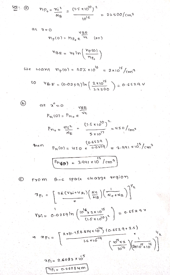
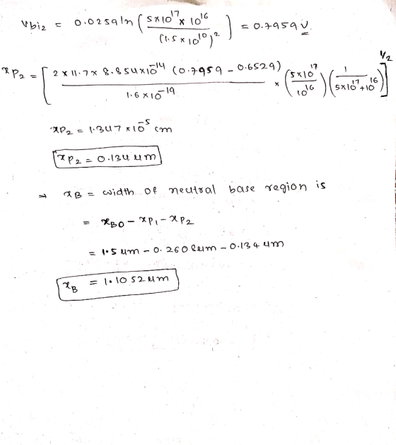
A uniformly doped silicon pnp transistor with base width of 2um is biased in forward active mode (with BC junction reverse biased). The doping concentrations are NE-1018cm NB-5x1016cm3, and Nc-1015cm...
 A uniformly doped silicon pnp transistor with base width of 2um is biased in forward active mode (with BC junction reverse biased). The doping concentrations are NE-1018cm NB-5x1016cm3, and Nc-1015cm3. Assume DB-25 cm2/s, TB-10-s and LB 16um (a) Calculate the values of no, рво, and nco. (b) For VEB 0.65V, determine the respective minority carrier concentration at the edge of the depletion layer, pa(0) and ne(0) (c) Sketch the minority carrier concentration through the device and label each curve (d)...
Consider a silicon device (which happens to be an npn bipolar transistor) with an emitter doping...
Consider a silicon device (which happens to be an npn bipolar transistor) with an emitter doping of 10^17/cm3, a base doping of 8x10^15/cm3 and a collector doping of 2x10^15/cm3. Carefully calculate how the band diagram, charge density, electric field and electrostatic potential as a function of distance for this device changes from the equilibrium case when this bipolar transistor is properly biased to work as an amplifier. In other words, show how the band diagram changes when the emitter-base junction...
2. (15 pts) An npn bipolar junction transistor is biased in the forward-active region. The common-base...
 2. (15 pts) An npn bipolar junction transistor is biased in the forward-active region. The common-base current gain, α 0.95. The input emitter current is IE-4.6 mA. a) Calculate the collector current Ic b) Calculate the common-emitter current gain, B c) Calculate the base current IB IB
Problem 2. A silicon NPN bipolar transistor has the following specifications: Emitter: N+: ND =1018 cm-3...
Problem 2. A silicon NPN bipolar transistor has the following specifications: Emitter: N+: ND =1018 cm-3 , base: p-type, NA=1015 cm-3, collector: N-type, ND=5x1015 cm-3 . 1. Draw the energy band diagram of the transistor at thermal equilibrium, 2. If the transistor is biased at Normal Active Mode, emitter-base junction forward biased with 1 V, and collector-base junction is reverse biased with 4V, draw the energy band diagram.
This problem pertains to silicon npn transistors biased in the normal active mode of operation at...
 This problem pertains to silicon npn transistors biased in the normal active mode of operation at T- 300 K. a) The emitter is doped 25 times more heavily than the base. The minority carrier mobility in the emitter is one-fourth that in the base. The base width is 15% of the minority camer diffusion length in the base. The minority carrier lifetimes in the base and emitter are identical. Calculate the base transport factor, emitter injection efficiency, ?, and ?...
Please answer and show all your work. Thank you! 6- A silicon pnp transistor has impurity...
 Please answer and show all your work. Thank you!
6- A silicon pnp transistor has impurity concentrations of 5 x 1018 cm3, 7 x 1016 cm-3, and 2 × 1016 cm-3 in the emitter, base and collector, respectively. The base width is 1.0 ?m, and the device cross-sectional area is 0.2 mm2. When the emitter-base junction is forward biased to 0.5 V and the base-collector junction is reverse biased to 5 V, calculate the neutral base width and the minority...
Please answer and show all your work. Thank you!
6- A silicon pnp transistor has impurity concentrations of 5 x 1018 cm3, 7 x 1016 cm-3, and 2 × 1016 cm-3 in the emitter, base and collector, respectively. The base width is 1.0 ?m, and the device cross-sectional area is 0.2 mm2. When the emitter-base junction is forward biased to 0.5 V and the base-collector junction is reverse biased to 5 V, calculate the neutral base width and the minority...
8.3 Consider a conventional NPN BJT with uniform doping. The base-emitter junction is forward biased, and...
 8.3 Consider a conventional NPN BJT with uniform doping. The base-emitter junction is forward biased, and the base-collector junction is reverse biased. (a) Qualitatively sketch the energy band diagram. (b) Sketch the minority carrier concentrations in the base, emitter, and collector regions. (c) List all the causes contributing to the base and collector currents. You may neglect thermal recombination-generation currents in the depletion regions.
Forward Active Reverse Active Cutoff Saturation 2. The minority carrier distribution in a NPN BJT under forward acti...
 Forward Active Reverse Active Cutoff Saturation 2. The minority carrier distribution in a NPN BJT under forward active bias is given in the following questions. On top of the figure, sketch the corresponding new minority carrier concentration when the given condition is changed. (To make the question simple, you may assume the depletion width remains unchanged in all questions. But you have to indicate the new equilibrium minority concentration if they are affected.) 6. a) collector doping is increased by...
question 3 and 4 Problem2 (30 points) Consider an npn bipolar transistor with the following characteristics...
 question 3 and 4
Problem2 (30 points) Consider an npn bipolar transistor with the following characteristics Base Collector Emitter Na-5x 1016 cm3 Ng- 1015 cm3 N1018 cm3 DC- 12 cm-/sec DE 8 cm-/sec (diff coef.) DB 15 cm-/sec sec TEO 108 sec (life time) tB0 5x 10 tCo 10 sec xp 0.7 um (Base width) xg 0.8 um (emitter width) D Remember D/u= KT /q, and L n.p n.p A forward bias of 0.5 V is applied to the emitter-base...
question 3 and 4
Problem2 (30 points) Consider an npn bipolar transistor with the following characteristics Base Collector Emitter Na-5x 1016 cm3 Ng- 1015 cm3 N1018 cm3 DC- 12 cm-/sec DE 8 cm-/sec (diff coef.) DB 15 cm-/sec sec TEO 108 sec (life time) tB0 5x 10 tCo 10 sec xp 0.7 um (Base width) xg 0.8 um (emitter width) D Remember D/u= KT /q, and L n.p n.p A forward bias of 0.5 V is applied to the emitter-base...
2. A silicon n'-p-n bipolar transistor has abrupt dopings of 1019, 3x10¹⁶, and 5x105 cm in...
 2. A silicon n'-p-n bipolar transistor has abrupt dopings of 1019, 3x10¹⁶, and 5x105 cm in the emitter, base, and collector, respectively. Find the upper limit of the base-collector voltage at which the emitter bias can no longer control the collector current (due to punch- through or avalanche breakdown). Assume the base width (between metallurgical junc- tions) is 0.5 um.
 A uniformly doped silicon pnp transistor with base width of 2um is biased in forward active mode (with BC junction reverse biased). The doping concentrations are NE-1018cm NB-5x1016cm3, and Nc-1015cm3. Assume DB-25 cm2/s, TB-10-s and LB 16um (a) Calculate the values of no, рво, and nco. (b) For VEB 0.65V, determine the respective minority carrier concentration at the edge of the depletion layer, pa(0) and ne(0) (c) Sketch the minority carrier concentration through the device and label each curve (d)...
 2. (15 pts) An npn bipolar junction transistor is biased in the forward-active region. The common-base current gain, α 0.95. The input emitter current is IE-4.6 mA. a) Calculate the collector current Ic b) Calculate the common-emitter current gain, B c) Calculate the base current IB IB
 This problem pertains to silicon npn transistors biased in the normal active mode of operation at T- 300 K. a) The emitter is doped 25 times more heavily than the base. The minority carrier mobility in the emitter is one-fourth that in the base. The base width is 15% of the minority camer diffusion length in the base. The minority carrier lifetimes in the base and emitter are identical. Calculate the base transport factor, emitter injection efficiency, ?, and ?...
 Please answer and show all your work. Thank you!
6- A silicon pnp transistor has impurity concentrations of 5 x 1018 cm3, 7 x 1016 cm-3, and 2 × 1016 cm-3 in the emitter, base and collector, respectively. The base width is 1.0 ?m, and the device cross-sectional area is 0.2 mm2. When the emitter-base junction is forward biased to 0.5 V and the base-collector junction is reverse biased to 5 V, calculate the neutral base width and the minority...
Please answer and show all your work. Thank you!
6- A silicon pnp transistor has impurity concentrations of 5 x 1018 cm3, 7 x 1016 cm-3, and 2 × 1016 cm-3 in the emitter, base and collector, respectively. The base width is 1.0 ?m, and the device cross-sectional area is 0.2 mm2. When the emitter-base junction is forward biased to 0.5 V and the base-collector junction is reverse biased to 5 V, calculate the neutral base width and the minority...
 8.3 Consider a conventional NPN BJT with uniform doping. The base-emitter junction is forward biased, and the base-collector junction is reverse biased. (a) Qualitatively sketch the energy band diagram. (b) Sketch the minority carrier concentrations in the base, emitter, and collector regions. (c) List all the causes contributing to the base and collector currents. You may neglect thermal recombination-generation currents in the depletion regions.
 Forward Active Reverse Active Cutoff Saturation 2. The minority carrier distribution in a NPN BJT under forward active bias is given in the following questions. On top of the figure, sketch the corresponding new minority carrier concentration when the given condition is changed. (To make the question simple, you may assume the depletion width remains unchanged in all questions. But you have to indicate the new equilibrium minority concentration if they are affected.) 6. a) collector doping is increased by...
 question 3 and 4
Problem2 (30 points) Consider an npn bipolar transistor with the following characteristics Base Collector Emitter Na-5x 1016 cm3 Ng- 1015 cm3 N1018 cm3 DC- 12 cm-/sec DE 8 cm-/sec (diff coef.) DB 15 cm-/sec sec TEO 108 sec (life time) tB0 5x 10 tCo 10 sec xp 0.7 um (Base width) xg 0.8 um (emitter width) D Remember D/u= KT /q, and L n.p n.p A forward bias of 0.5 V is applied to the emitter-base...
question 3 and 4
Problem2 (30 points) Consider an npn bipolar transistor with the following characteristics Base Collector Emitter Na-5x 1016 cm3 Ng- 1015 cm3 N1018 cm3 DC- 12 cm-/sec DE 8 cm-/sec (diff coef.) DB 15 cm-/sec sec TEO 108 sec (life time) tB0 5x 10 tCo 10 sec xp 0.7 um (Base width) xg 0.8 um (emitter width) D Remember D/u= KT /q, and L n.p n.p A forward bias of 0.5 V is applied to the emitter-base...
 2. A silicon n'-p-n bipolar transistor has abrupt dopings of 1019, 3x10¹⁶, and 5x105 cm in the emitter, base, and collector, respectively. Find the upper limit of the base-collector voltage at which the emitter bias can no longer control the collector current (due to punch- through or avalanche breakdown). Assume the base width (between metallurgical junc- tions) is 0.5 um.
Most questions answered within 3 hours.
-
Why do organizations decline? What steps can top
management take to halt, decline, and restore organizational...
asked 43 minutes ago -
. Suppose a discrete random variable has probability
distribution
P(x) = .2 if x = 0...
asked 29 minutes ago -
Under the influence of its drive force, a snowmobile is moving
at a constant velocity along...
asked 58 minutes ago -
What mechanisms Drive speciation??
(I.e. what was Dawins theory on the orgin of species, and how...
asked 2 hours ago -
The manager at a car assembly plant believes that the mean
assembly time for a car...
asked 3 hours ago -
Which of the following is true of electron capture?
A) It decreases the nuclide's mass number...
asked 4 hours ago -
Assuming an efficiency of 43.10%, calculate the actual yield of
magnesium nitrate formed from 114.9 g...
asked 5 hours ago -
The highly pathogenic bacterium Clostridium
perfringens causes gangrene, a disease that results in the
destruction of...
asked 7 hours ago -
In the context of situation analysis, which of the following is
a category for analysis in...
asked 7 hours ago -
In a study of the gas phase decomposition of sulfuryl chloride
at 600 K SO2Cl2(g)SO2(g) +...
asked 7 hours ago -
75 g of 2-propanol (C3H8O) and 25 g of pentane are mixed in a
200 mL...
asked 7 hours ago -
The 2800-turn coil in a dc motor has an area per turn of 1.1 ×
10-2...
asked 7 hours ago