
Homework Answers
Add Answer to:
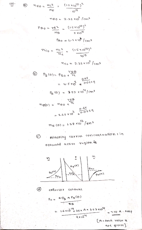
A uniformly doped silicon pnp transistor with base width of 2um is biased in forward active mode (with BC junction reverse biased). The doping concentrations are NE-1018cm NB-5x1016cm3, and Nc-1015cm...
3. A silicon npn bipolar transistor is uniformly doped and biased in the forward active region wi...
 3. A silicon npn bipolar transistor is uniformly doped and biased in the forward active region with the base-collector junction reverse biased by 2.5 V. The metallurgical base width is 1.5 μm. The emitter, base collector doping concentrations are 5 × 10¹⁷, 1016, 2 × 1015 cm-3 respectively. a. At T-300 K, calculate the base-emitter voltage at which the minority carrier electron concentration at x-0 is 20% of the majority carrier hole concentration. At this voltage calculate the minority carrier...
8.3 Consider a conventional NPN BJT with uniform doping. The base-emitter junction is forward biased, and...
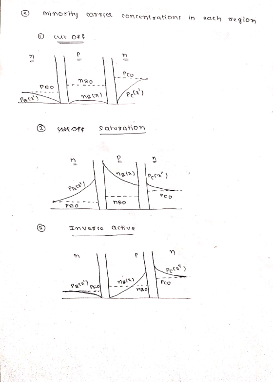
 8.3 Consider a conventional NPN BJT with uniform doping. The base-emitter junction is forward biased, and the base-collector junction is reverse biased. (a) Qualitatively sketch the energy band diagram. (b) Sketch the minority carrier concentrations in the base, emitter, and collector regions. (c) List all the causes contributing to the base and collector currents. You may neglect thermal recombination-generation currents in the depletion regions.
Please answer and show all your work. Thank you! 6- A silicon pnp transistor has impurity...
 Please answer and show all your work. Thank you!
6- A silicon pnp transistor has impurity concentrations of 5 x 1018 cm3, 7 x 1016 cm-3, and 2 × 1016 cm-3 in the emitter, base and collector, respectively. The base width is 1.0 ?m, and the device cross-sectional area is 0.2 mm2. When the emitter-base junction is forward biased to 0.5 V and the base-collector junction is reverse biased to 5 V, calculate the neutral base width and the minority...
Please answer and show all your work. Thank you!
6- A silicon pnp transistor has impurity concentrations of 5 x 1018 cm3, 7 x 1016 cm-3, and 2 × 1016 cm-3 in the emitter, base and collector, respectively. The base width is 1.0 ?m, and the device cross-sectional area is 0.2 mm2. When the emitter-base junction is forward biased to 0.5 V and the base-collector junction is reverse biased to 5 V, calculate the neutral base width and the minority...
 3. A silicon npn bipolar transistor is uniformly doped and biased in the forward active region with the base-collector junction reverse biased by 2.5 V. The metallurgical base width is 1.5 μm. The emitter, base collector doping concentrations are 5 × 10¹⁷, 1016, 2 × 1015 cm-3 respectively. a. At T-300 K, calculate the base-emitter voltage at which the minority carrier electron concentration at x-0 is 20% of the majority carrier hole concentration. At this voltage calculate the minority carrier...
 8.3 Consider a conventional NPN BJT with uniform doping. The base-emitter junction is forward biased, and the base-collector junction is reverse biased. (a) Qualitatively sketch the energy band diagram. (b) Sketch the minority carrier concentrations in the base, emitter, and collector regions. (c) List all the causes contributing to the base and collector currents. You may neglect thermal recombination-generation currents in the depletion regions.
 Please answer and show all your work. Thank you!
6- A silicon pnp transistor has impurity concentrations of 5 x 1018 cm3, 7 x 1016 cm-3, and 2 × 1016 cm-3 in the emitter, base and collector, respectively. The base width is 1.0 ?m, and the device cross-sectional area is 0.2 mm2. When the emitter-base junction is forward biased to 0.5 V and the base-collector junction is reverse biased to 5 V, calculate the neutral base width and the minority...
Please answer and show all your work. Thank you!
6- A silicon pnp transistor has impurity concentrations of 5 x 1018 cm3, 7 x 1016 cm-3, and 2 × 1016 cm-3 in the emitter, base and collector, respectively. The base width is 1.0 ?m, and the device cross-sectional area is 0.2 mm2. When the emitter-base junction is forward biased to 0.5 V and the base-collector junction is reverse biased to 5 V, calculate the neutral base width and the minority...
Most questions answered within 3 hours.
-
The average length of time between arrivals at a turnpike
toll-booth is 26 seconds. What is...
asked 45 minutes ago -
(a) A piston at 6.1 atm contains a gas that occupies a volume of
3.5 L....
asked 1 hour ago -
Please answer true or false. Words
cannot be changed or added in to make it true...
asked 1 hour ago -
An empty test tube weighs 15.923 grams. Then,
MgCl2•6H2O is added into the test tube. After...
asked 1 hour ago -
Assume memory access is 10 units of time and disk access is
10000 units of time....
asked 2 hours ago -
1. Are all good samples random?
2. Magazines often report surveys giving statistics such as “63%...
asked 2 hours ago -
Under all the various types of market structures, firms
must eventually earn some economic profits for...
asked 2 hours ago -
Consider the following fitness regime for a single locus trait
with two co-dominant alleles: w11 =...
asked 2 hours ago -
A large cable company reports the following.
80% of its customers subscribe to its cable TV...
asked 2 hours ago -
Please answer the question in brief.
Discuss the role of ERP in organizations. Are ERP tools...
asked 2 hours ago -
Discuss the pros and cons of collaborative software such
as SameTime. Does it increase productivity? What...
asked 2 hours ago -
Buying your in-laws a gift because it’s expected is
due to the ____________ motive of gift-giving....
asked 2 hours ago