
Homework Answers


Add Answer to:
Problem1 10" ㎝aandn-side Callibrium at 3000 K has ap side dup ing of NA-2 doping of ND-101 cm Ca...
A Si step junction maintained at room temperature under equilibrium conditions has a p-side doping of...
A Si step junction maintained at room temperature under equilibrium conditions has a p-side doping of Na = 2x10¹⁵/cm3 , and an n-side doping of Nd = 1015/cm3 . Compute (a) Built-in potential Vbi (b) Depletion region width W, and xp, xn (c) Maximum electric field at x=0 (d) Electrostatic potential V at x=0 (e) Make sketches of the charge density, electric field, and electrostatic potential as a function of position x
Q1) A diode has a doping of No- 1019 /cm3 on the n-type side and NA 101/cm3 on the p-type side. W...
 Q1) A diode has a doping of No- 1019 /cm3 on the n-type side and NA 101/cm3 on the p-type side. What are the a) width of depletion region, b) width of depletion region in n side, c) width of depletion region in p side, d) junction potential at zero bias, e) junction width at a reverse bias of 13 V, and f) maximum electric field in zero bias just in the middle of the P-N junction at room temperature?...
1. (2) A Si p-n junction has sides with boron doping at 107 cm and phosphorus...
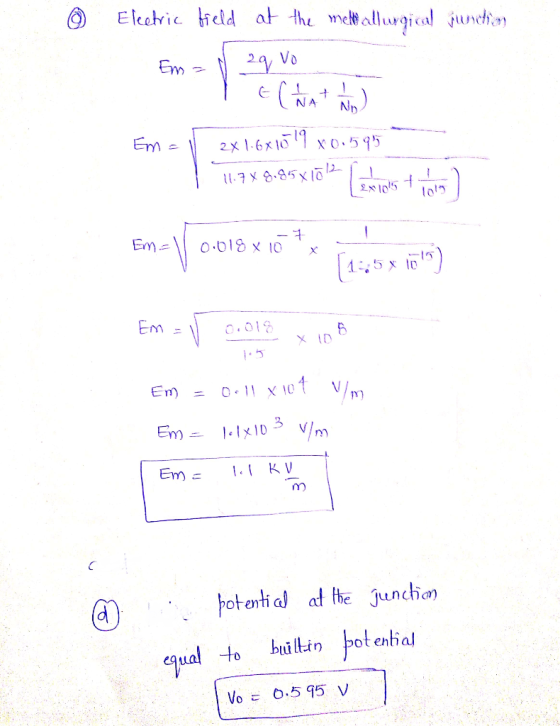
 1. (2) A Si p-n junction has sides with boron doping at 107 cm and phosphorus doping at 5.0x10^? cm? The junction has a cross-sectional area of 104 cm. It is in equilibrium at a temperature of 300 K. For Si, the intrinsic charge carrier density is 1.5x100 cm and the dielectric constant is 11.8. State the contact potential, the total depletion region width, the depletion region widths on the p-side and n- side, and the peak electric field. What...
A p-n junction is created by doping the right side of a piece of silicon with...
A p-n junction is created by doping the right side of a piece of silicon with 1014 atoms/cm3 of phosphorus and the left side with 1018 atoms/cm3 of boron. Assume that the dopants are fully ionized, and assume the junction is at x = 0 with x+ pointed to the right. a) Plot by hand (roughly to scale) an energy band diagram of the junction and label EGAP, EC, EV, EF and EFi. Using the effective density of states, calculate...
A p-i-n junction has an intrinsic region thickness of 1-um (micrometer) The p side has Na...
A p-i-n junction has an intrinsic region thickness of 1-um (micrometer) The p side has Na =10^15 and the n side has Nd=10^19. a) Derive the electric field and potential using Poisson's equation. b) Calculate the depletion region width (take into account the 1-um and the depletion region width for a regular pn junction)
(iv) [2 Marks] A pn-junction has a built-in potential voltage of 1V across the junction. The width of the depletion reg...
 (iv) [2 Marks] A pn-junction has a built-in potential voltage of 1V across the junction. The width of the depletion region is 1um. The acceptor doping is NA 2 x 1015cm-3 in the P-side and a donor doping is Np = 8 x 1015cm-3 on the N-side. If the reference position x 0 is the edge of the depletion region on the P-side and the P region is on the left of the N region then where does the maximum...
4.1* An abrupt silicon pn junction has dopant con- centrations of Na = 1 1015 cm-3...
 4.1* An abrupt silicon pn junction has dopant con- centrations of Na = 1 1015 cm-3 and Na = 2 x 107 cm3. (a) Evaluate the built-in potential d; at room tem- perature. (b) Using the depletion approximation, calculate the width of the space-charge layer and the peak electric field for junction voltages Ve equal to 0 V and -10 V.
 Q1) A diode has a doping of No- 1019 /cm3 on the n-type side and NA 101/cm3 on the p-type side. What are the a) width of depletion region, b) width of depletion region in n side, c) width of depletion region in p side, d) junction potential at zero bias, e) junction width at a reverse bias of 13 V, and f) maximum electric field in zero bias just in the middle of the P-N junction at room temperature?...
 1. (2) A Si p-n junction has sides with boron doping at 107 cm and phosphorus doping at 5.0x10^? cm? The junction has a cross-sectional area of 104 cm. It is in equilibrium at a temperature of 300 K. For Si, the intrinsic charge carrier density is 1.5x100 cm and the dielectric constant is 11.8. State the contact potential, the total depletion region width, the depletion region widths on the p-side and n- side, and the peak electric field. What...
 (iv) [2 Marks] A pn-junction has a built-in potential voltage of 1V across the junction. The width of the depletion region is 1um. The acceptor doping is NA 2 x 1015cm-3 in the P-side and a donor doping is Np = 8 x 1015cm-3 on the N-side. If the reference position x 0 is the edge of the depletion region on the P-side and the P region is on the left of the N region then where does the maximum...
 4.1* An abrupt silicon pn junction has dopant con- centrations of Na = 1 1015 cm-3 and Na = 2 x 107 cm3. (a) Evaluate the built-in potential d; at room tem- perature. (b) Using the depletion approximation, calculate the width of the space-charge layer and the peak electric field for junction voltages Ve equal to 0 V and -10 V.
Most questions answered within 3 hours.
-
han discusses the racist practice of badlands, a bar
in the Castro
district of San Francisco,...
asked 5 minutes ago -
A sample of final exam scores is normally distributed with a
mean equal to 25 and...
asked 8 minutes ago -
An investor shorts 100 shares of a stock when the share price is
$50 and closes...
asked 12 minutes ago -
LLOP corporation just paid 4$ dividend per share, you expect the
dividend to grow 8% for...
asked 21 minutes ago -
if we subtract 1000 from 0001 is there overflow? (binary)
asked 30 minutes ago -
Hello, I need help with the function below, The language I am
using is Ocaml
open...
asked 31 minutes ago -
Explain how the presence of glucose represses the gal structural
genes?
asked 39 minutes ago -
For the reaction CaI2+2AgNO3⟶2AgI+Ca(NO3)2 how many grams of
silver iodide, AgI, are produced from 56.5 g...
asked 50 minutes ago -
Write an equation for hydrolysis via acid catalysis.
Using ethyl acetate, ethyl benzoate, ethyl formate or...
asked 58 minutes ago -
Only one graph is needed.
(a) Draw a Supply Curve and the Demand Curve for the...
asked 1 hour ago -
Fill in the blanks and please show how you arrived at numerical
answers
. The...
asked 1 hour ago -
91. If the half – life of a sample of radioactive
material is 60 days, what...
asked 1 hour ago