What is the voltage stress on the switch S1 when it is
off, and what is the voltage stress on the diode D1 when it is off?
Derive the equations based on the input voltage, the output
voltage, and the turns-ratio of the transformer. Draw the
equivalent circuits. Solve for the case when, vIN = 15 V,
N1/N2 = 2, and D = 0.4
Homework Answers

Add Answer to:
What is the voltage stress on the switch S1 when it is off, and what is the voltage stress on the...
QUESTION; Find maximum voltage stress of the switch in the primary winding and diode in the...
QUESTION; Find maximum voltage stress of the switch in the primary winding and diode in the tertiary winding if the converter-transformer has 10 primary turns and 15 tertiary turns and the maximum input dc voltage is 300 volts.
(c) The dual-switch forward converter in Fig. Q4(c) is supplied from an input voltage Vin of 42V,...
 (c) The dual-switch forward converter in Fig. Q4(c) is supplied from an input voltage Vin of 42V, and switches at 100kHz with a duty factor of 0.35. The transformer T1 carries 50 primary turns and 34 secondary turns. The core used in T1 has an effective area of 45mm2 and an effective length of 72mm. The relative permeability of its core material is =1790. [NB: The permeability of free space IS μ.-1.257×10-94/m.] V.D D, L1 TRI - 01 N1 N2...
Design a flyback converter for an input of 24 volts and an output of 40 volts. Assume a 40W load and keep the blocking voltage for the transistor to < 26 volts. For your design determine: a) The tr...
 Design a flyback converter for an input of 24 volts and an
output of 40 volts. Assume a 40W load and keep the blocking voltage
for the transistor to < 26 volts.
For your design determine:
a) The transformer turn ratio n (5).
b) The duty cycle D (5).
c) The average source current (3).
d) The output voltage of the converter when we include the
effect of a transformer winding losses as 0.05 ohms (7).
Using a MOSFET and...
Design a flyback converter for an input of 24 volts and an
output of 40 volts. Assume a 40W load and keep the blocking voltage
for the transistor to < 26 volts.
For your design determine:
a) The transformer turn ratio n (5).
b) The duty cycle D (5).
c) The average source current (3).
d) The output voltage of the converter when we include the
effect of a transformer winding losses as 0.05 ohms (7).
Using a MOSFET and...
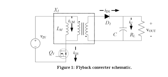
Question 1 For the flyback converter shown in Fig. 1, Vin is 30 V, Vout is 8 V, the output power is 30 w, 30 turns are...
 Question 1 For the flyback converter shown in Fig. 1, Vin is 30 V, Vout is 8 V, the output power is 30 w, 30 turns are fitted to winding Ww1, 15 turns are fitted to winding W2, the inductance of W1, L1, is 50 uH and the switching frequency is 200 kHz. The flyback converter operates in continuous conduction mode. Calculate the time for which S1 is switched on a. b. Calculate Aisı during the time S1 is switched...
In this part of the term paper, design a single-phase switch-mode DC power supply with a forward ...
 In this part of the term paper, design a single-phase switch-mode DC power supply with a forward converter. Provide answers to the questions below Please combine the single-phase full-wave rectifier from part two of your term paper with a forward converter to produce a switch-mode DC power supply, as shown below. The output of the bridge rectifier serves as input to the forward converter L1 Np: N BH621BH62 D, V1 Load C1 100p 45 Vrms D3 BH62 18H62 D4 Control...
The following circuit is a buck-boost converter where M1 functions as a switch. a. Describe how...
 The following circuit is a buck-boost converter where M1 functions as a switch. a. Describe how the converter works when M1 is switched on and off. b. Provide proof that V where D is the duty cycle controlled by the MOSFET, M1. 1-D Ignore the voltage drop across the transistor and the diode. D1 Vin C1 Gate drive circuit L1 RL c. Plot the transistor current, the inductor current, the capacitor current, and the load current as a function of...
I want to solve this problem step by step 1. (35 points) Switch mode DC / DC Converters. a. (15 points) Design a flyback DC/DC power converter to the following specifications. Assume ideal compone...
 I want to solve this problem step by step
1. (35 points) Switch mode DC / DC Converters. a. (15 points) Design a flyback DC/DC power converter to the following specifications. Assume ideal components. Input Voltage Output Voltage Output Power Switching frequency Maximum Current Ripple in the filter inductor Output ripple voltage: Continuous conduction 170 VDC 12 VDC 40 Watts 750 kHz 1.2 Amps Your answer should include a circuit diagram with each energy storage element labeled with its value....
I want to solve this problem step by step
1. (35 points) Switch mode DC / DC Converters. a. (15 points) Design a flyback DC/DC power converter to the following specifications. Assume ideal components. Input Voltage Output Voltage Output Power Switching frequency Maximum Current Ripple in the filter inductor Output ripple voltage: Continuous conduction 170 VDC 12 VDC 40 Watts 750 kHz 1.2 Amps Your answer should include a circuit diagram with each energy storage element labeled with its value....
Please, need help to do this. the mode is DCM mode. Problem 2.1 Sketch the current and voltage waveforms of: the in...
 Please, need help to do this. the mode is DCM mode.
Problem 2.1 Sketch the current and voltage waveforms of: the inductor current ((t)), the inductor voltage (v(t)) the input current (is(t)), the output diode current (ip2(t)), and the output capacitor current (ico(t)), for at least one full period T when the Buck-Boost converter is operating in Discontinuous conduction Mode (DCM). Assume that the converter is lossless, or 100% efficient, that is: The switch ON-resistance is on, and both the...
Please, need help to do this. the mode is DCM mode.
Problem 2.1 Sketch the current and voltage waveforms of: the inductor current ((t)), the inductor voltage (v(t)) the input current (is(t)), the output diode current (ip2(t)), and the output capacitor current (ico(t)), for at least one full period T when the Buck-Boost converter is operating in Discontinuous conduction Mode (DCM). Assume that the converter is lossless, or 100% efficient, that is: The switch ON-resistance is on, and both the...
can you show where to measure, the quantity listed in the pic? like what two points...
 can you show where to measure, the quantity listed in the
pic?
like what two points to get the answer
for
all of them, please.
In this step, you will add a second transistor, causing the switching action to improve dramatically. The circuit is shown in Figure 10-2. Notice that the 1.0 k resistor is now the collector resistor for Q. The circuit works as follows. When Vw is very low, Q, is off since it does not have sufficient...
can you show where to measure, the quantity listed in the
pic?
like what two points to get the answer
for
all of them, please.
In this step, you will add a second transistor, causing the switching action to improve dramatically. The circuit is shown in Figure 10-2. Notice that the 1.0 k resistor is now the collector resistor for Q. The circuit works as follows. When Vw is very low, Q, is off since it does not have sufficient...
1. Why can the DSO only measure node voltages when the Function Generator is the power supply in ...
 1. Why can the DSO only measure node voltages when the Function Generator is the power supply in a circuit (unless it is using a current probe)? 2. Consider Figure 1. According to the calculations in the lab handout, if Z-1kΩ +/6914, then the phase difference (фи-фі) between u(t) and i (t) is 34.6". a. If this v(t) and i(t) were displayed on a DSO (v(t) being a node voltage and using a current probe for i(t) as shown in...
 (c) The dual-switch forward converter in Fig. Q4(c) is supplied from an input voltage Vin of 42V, and switches at 100kHz with a duty factor of 0.35. The transformer T1 carries 50 primary turns and 34 secondary turns. The core used in T1 has an effective area of 45mm2 and an effective length of 72mm. The relative permeability of its core material is =1790. [NB: The permeability of free space IS μ.-1.257×10-94/m.] V.D D, L1 TRI - 01 N1 N2...
 Design a flyback converter for an input of 24 volts and an
output of 40 volts. Assume a 40W load and keep the blocking voltage
for the transistor to < 26 volts.
For your design determine:
a) The transformer turn ratio n (5).
b) The duty cycle D (5).
c) The average source current (3).
d) The output voltage of the converter when we include the
effect of a transformer winding losses as 0.05 ohms (7).
Using a MOSFET and...
Design a flyback converter for an input of 24 volts and an
output of 40 volts. Assume a 40W load and keep the blocking voltage
for the transistor to < 26 volts.
For your design determine:
a) The transformer turn ratio n (5).
b) The duty cycle D (5).
c) The average source current (3).
d) The output voltage of the converter when we include the
effect of a transformer winding losses as 0.05 ohms (7).
Using a MOSFET and...
 Question 1 For the flyback converter shown in Fig. 1, Vin is 30 V, Vout is 8 V, the output power is 30 w, 30 turns are fitted to winding Ww1, 15 turns are fitted to winding W2, the inductance of W1, L1, is 50 uH and the switching frequency is 200 kHz. The flyback converter operates in continuous conduction mode. Calculate the time for which S1 is switched on a. b. Calculate Aisı during the time S1 is switched...
 In this part of the term paper, design a single-phase switch-mode DC power supply with a forward converter. Provide answers to the questions below Please combine the single-phase full-wave rectifier from part two of your term paper with a forward converter to produce a switch-mode DC power supply, as shown below. The output of the bridge rectifier serves as input to the forward converter L1 Np: N BH621BH62 D, V1 Load C1 100p 45 Vrms D3 BH62 18H62 D4 Control...
 The following circuit is a buck-boost converter where M1 functions as a switch. a. Describe how the converter works when M1 is switched on and off. b. Provide proof that V where D is the duty cycle controlled by the MOSFET, M1. 1-D Ignore the voltage drop across the transistor and the diode. D1 Vin C1 Gate drive circuit L1 RL c. Plot the transistor current, the inductor current, the capacitor current, and the load current as a function of...
 I want to solve this problem step by step
1. (35 points) Switch mode DC / DC Converters. a. (15 points) Design a flyback DC/DC power converter to the following specifications. Assume ideal components. Input Voltage Output Voltage Output Power Switching frequency Maximum Current Ripple in the filter inductor Output ripple voltage: Continuous conduction 170 VDC 12 VDC 40 Watts 750 kHz 1.2 Amps Your answer should include a circuit diagram with each energy storage element labeled with its value....
I want to solve this problem step by step
1. (35 points) Switch mode DC / DC Converters. a. (15 points) Design a flyback DC/DC power converter to the following specifications. Assume ideal components. Input Voltage Output Voltage Output Power Switching frequency Maximum Current Ripple in the filter inductor Output ripple voltage: Continuous conduction 170 VDC 12 VDC 40 Watts 750 kHz 1.2 Amps Your answer should include a circuit diagram with each energy storage element labeled with its value....
 Please, need help to do this. the mode is DCM mode.
Problem 2.1 Sketch the current and voltage waveforms of: the inductor current ((t)), the inductor voltage (v(t)) the input current (is(t)), the output diode current (ip2(t)), and the output capacitor current (ico(t)), for at least one full period T when the Buck-Boost converter is operating in Discontinuous conduction Mode (DCM). Assume that the converter is lossless, or 100% efficient, that is: The switch ON-resistance is on, and both the...
Please, need help to do this. the mode is DCM mode.
Problem 2.1 Sketch the current and voltage waveforms of: the inductor current ((t)), the inductor voltage (v(t)) the input current (is(t)), the output diode current (ip2(t)), and the output capacitor current (ico(t)), for at least one full period T when the Buck-Boost converter is operating in Discontinuous conduction Mode (DCM). Assume that the converter is lossless, or 100% efficient, that is: The switch ON-resistance is on, and both the...
 can you show where to measure, the quantity listed in the
pic?
like what two points to get the answer
for
all of them, please.
In this step, you will add a second transistor, causing the switching action to improve dramatically. The circuit is shown in Figure 10-2. Notice that the 1.0 k resistor is now the collector resistor for Q. The circuit works as follows. When Vw is very low, Q, is off since it does not have sufficient...
can you show where to measure, the quantity listed in the
pic?
like what two points to get the answer
for
all of them, please.
In this step, you will add a second transistor, causing the switching action to improve dramatically. The circuit is shown in Figure 10-2. Notice that the 1.0 k resistor is now the collector resistor for Q. The circuit works as follows. When Vw is very low, Q, is off since it does not have sufficient...
 1. Why can the DSO only measure node voltages when the Function Generator is the power supply in a circuit (unless it is using a current probe)? 2. Consider Figure 1. According to the calculations in the lab handout, if Z-1kΩ +/6914, then the phase difference (фи-фі) between u(t) and i (t) is 34.6". a. If this v(t) and i(t) were displayed on a DSO (v(t) being a node voltage and using a current probe for i(t) as shown in...
Most questions answered within 3 hours.
-
Minitab Problem: Take the Lake Hume June rainfall data and find
use the processes outlined in...
asked 37 minutes ago -
X Company is trying to decide whether to continue using old
equipment to make Product A...
asked 38 minutes ago -
IN PYTHON ONLY !! Program 2: Re-work
program #5 (WeeklyHours) from the previous assignment such that...
asked 1 hour ago -
The average length of time between arrivals at a turnpike
toll-booth is 26 seconds. What is...
asked 2 hours ago -
(a) A piston at 6.1 atm contains a gas that occupies a volume of
3.5 L....
asked 4 hours ago -
Please answer true or false. Words
cannot be changed or added in to make it true...
asked 4 hours ago -
An empty test tube weighs 15.923 grams. Then,
MgCl2•6H2O is added into the test tube. After...
asked 4 hours ago -
Assume memory access is 10 units of time and disk access is
10000 units of time....
asked 4 hours ago -
1. Are all good samples random?
2. Magazines often report surveys giving statistics such as “63%...
asked 4 hours ago -
Under all the various types of market structures, firms
must eventually earn some economic profits for...
asked 4 hours ago -
Consider the following fitness regime for a single locus trait
with two co-dominant alleles: w11 =...
asked 4 hours ago -
A large cable company reports the following.
80% of its customers subscribe to its cable TV...
asked 4 hours ago