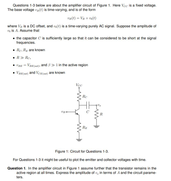

QUESTION 1 Find the answer to Question 1 (in volt) in the attached pdf file, where Vcc 20 volt VB 9 volt Rc 6.1 k-Ohm RE 1.6 k-Ohm A 1.1 volt VBE(sat) 0.6 volt VCE(sat) 0.2 volt Please round your answer to 3 decimal places.
Homework Answers


Add Answer to:
It Kind of goes without saying but if you have no knowledge than dont comment or try and answer this question you dope Questions 1-3 below are about the amplifier circuit of Figure 1. Here Vcc is a...
In the amplifier circuit in Figure 1 assume further that the transistor remains in the active region at all times. Express the amplitude of "vo" in terms of A and the circuit parameters. Plea...
 In the amplifier circuit in Figure 1 assume further that the
transistor remains in the active region at all times. Express the
amplitude of "vo" in terms of A and the circuit parameters. Please
express algebraically.
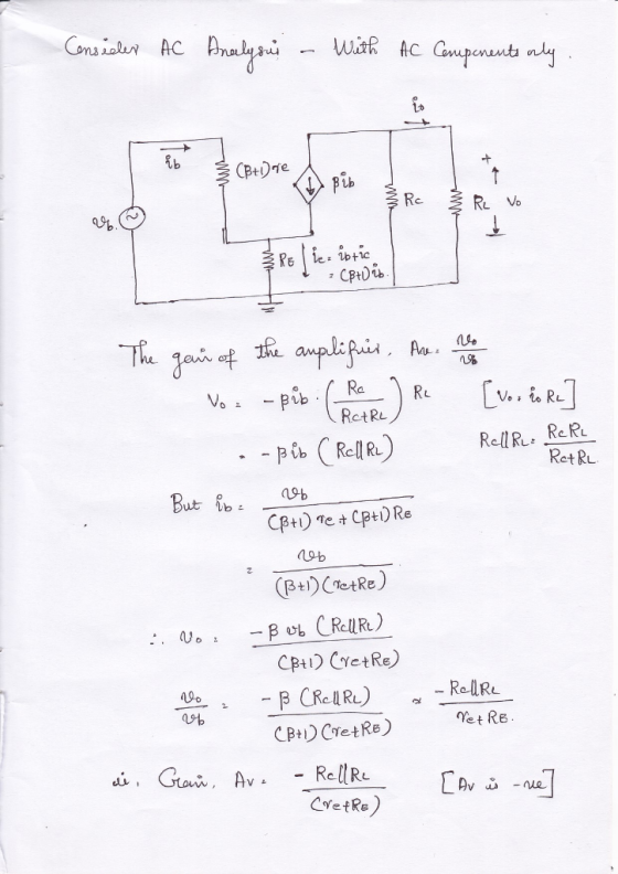
where Ve is a DC offset, and vb(t) is a time-varying purely AC signal. Suppose the amplitude of vb is A. Assume that the capacitor C is sufficiently large so that it can be considered to be short at the signal frequencies. . Rc,...
In the amplifier circuit in Figure 1 assume further that the
transistor remains in the active region at all times. Express the
amplitude of "vo" in terms of A and the circuit parameters. Please
express algebraically.
where Ve is a DC offset, and vb(t) is a time-varying purely AC signal. Suppose the amplitude of vb is A. Assume that the capacitor C is sufficiently large so that it can be considered to be short at the signal frequencies. . Rc,...
5. (20 points) For the amplifier in the following figure: +Vcc Rout Rc C3 R2 Rin Ri 1 k R3 Vo Vi R1 RE -VEE a) Draw the de equivalent circuit and find the Q-point. Assume B -75 b) Draw the equiv...
 5. (20 points) For the amplifier in the following figure: +Vcc Rout Rc C3 R2 Rin Ri 1 k R3 Vo Vi R1 RE -VEE a) Draw the de equivalent circuit and find the Q-point. Assume B -75 b) Draw the equivalent circuit used for ac analysis. Find the values in Thevenin equivalent representation for the amplifiers between C, and C as shown below. What is the maximum value of v, that satisfies the small- signal assumption? Rout Ri vi...
Hi everyone, I have a question about active filter, including a simulation, Please provide the sc...
 Hi everyone, I have a question about active filter, including a
simulation,
Please provide the screen capture.
Thanks.
5. Active Filter - III Consider the RC op-amp circuit shown in Fig. 5.4. Vin(t) is a sinusoidal signal with Vpp = 1 V, Rı = 10 ㏀ , R, = 20 ㏀ , and C,-C,-0.01 μF. Use Vcc-15V, The capacitors have zero initial energy stored. Ri 741 C1 C2 Volt) Fig. 5.5: Active filter - III (a) Find the transfer function...
Hi everyone, I have a question about active filter, including a
simulation,
Please provide the screen capture.
Thanks.
5. Active Filter - III Consider the RC op-amp circuit shown in Fig. 5.4. Vin(t) is a sinusoidal signal with Vpp = 1 V, Rı = 10 ㏀ , R, = 20 ㏀ , and C,-C,-0.01 μF. Use Vcc-15V, The capacitors have zero initial energy stored. Ri 741 C1 C2 Volt) Fig. 5.5: Active filter - III (a) Find the transfer function...
please pick one of the multiple choice options above. show all work, thank you Question 9...
 please pick one of the multiple choice options above.
show all work, thank you
Question 9 CIRCUIT X/FIG.9 (5 Marks) Statement: Consider the RC-coupled amplifier circuit illustrated in Fig. 9 (CIRCUIT X). Sketching relevant output (Vc-Ic) characteristics that decide Q-point coordinates and DC load-line details (of the NPN-BJT/Si circuit of Fig. 9 of Circuit X) Further, establish an appropriate AC-load line and decide the maximum swing of the output voltage across Rload with respect to the Q-point. Assume the input...
please pick one of the multiple choice options above.
show all work, thank you
Question 9 CIRCUIT X/FIG.9 (5 Marks) Statement: Consider the RC-coupled amplifier circuit illustrated in Fig. 9 (CIRCUIT X). Sketching relevant output (Vc-Ic) characteristics that decide Q-point coordinates and DC load-line details (of the NPN-BJT/Si circuit of Fig. 9 of Circuit X) Further, establish an appropriate AC-load line and decide the maximum swing of the output voltage across Rload with respect to the Q-point. Assume the input...
Laboratory 2: Transistor circuit characteristics A. Objectives: 1. To study the basic characteris...
 Laboratory 2: Transistor circuit characteristics A. Objectives: 1. To study the basic characteristics of a transistor circuit. 2. To study the bias circuit of a transistor circuit. B. Apparatus: 1. DC Power supply 2. Experimental boards and corresponding components 3. Electronic calculator (prepared by students) 4. Digital camera (prepared by students for photo taking of the experimental results) 5. Laptop computer with the software PicoScope 6 and Microsoft Word installed. 6. PicoScope PC Oscilloscope and its accessories. 7. Digital multi-meter....
Design a BJT amplifier based on the specifications provided in the table below. Your design shoul...
 THE STEPS TO DO SO:
Design a BJT amplifier based on the specifications provided in the table below. Your design should be insensitive to β variations, and both the input and the output should be AC coupled as in Fig. 1. Supply Voltage, Vcc Load Resistance, RL Transistor's Current Gain, β Relative Variation of lc for VBE-0.7 ± 0.1 V 0-to-Peak Output Swing, Vo Voltage Gain, A Input Resistance, R THD for 5kHz IV (0-to-peak) Sine Wave Output Voltage, V。S5%...
THE STEPS TO DO SO:
Design a BJT amplifier based on the specifications provided in the table below. Your design should be insensitive to β variations, and both the input and the output should be AC coupled as in Fig. 1. Supply Voltage, Vcc Load Resistance, RL Transistor's Current Gain, β Relative Variation of lc for VBE-0.7 ± 0.1 V 0-to-Peak Output Swing, Vo Voltage Gain, A Input Resistance, R THD for 5kHz IV (0-to-peak) Sine Wave Output Voltage, V。S5%...
1-Clear handwriting 2-Correct answer 3-Organized 4-answer all the questions Please Problem 2 On the circuit on...
 1-Clear handwriting
2-Correct answer
3-Organized
4-answer all the questions
Please
Problem 2 On the circuit on Figure P2, transi stor Q1 has a threshold voltage of Vt = 2 V and a transconductance parameter of k = 100 mA/V2. Note that Vcc = -Vee = 4.5 V. Moreover, capacitors C1, C2, and C3 can be assumed to be very large VDD 4.5.0 R3 25kQ R1 300kn C2 Vout C1 Rsig Q1 1k0 R2 200kn Vsig (R4 2kQ C3 -4.5V VSS...
1-Clear handwriting
2-Correct answer
3-Organized
4-answer all the questions
Please
Problem 2 On the circuit on Figure P2, transi stor Q1 has a threshold voltage of Vt = 2 V and a transconductance parameter of k = 100 mA/V2. Note that Vcc = -Vee = 4.5 V. Moreover, capacitors C1, C2, and C3 can be assumed to be very large VDD 4.5.0 R3 25kQ R1 300kn C2 Vout C1 Rsig Q1 1k0 R2 200kn Vsig (R4 2kQ C3 -4.5V VSS...
can someone help me with part c mpt tope alswersol the sdme part of you willbe penalized for this. Question 1 1 pts For the circuit shown in Figure 6.49, let Vcc -9V.RE 0.11 kQ, R1 3.6 k2, R2 5.6...
 can someone help me with part c
mpt tope alswersol the sdme part of you willbe penalized for this. Question 1 1 pts For the circuit shown in Figure 6.49, let Vcc -9V.RE 0.11 kQ, R1 3.6 k2, R2 5.6k(2, and Rs -o Ω . The transistor parameters are β-200. VBE(On)-Q7V, VA - 100 V and VT 0.026 V.(a) Determine the quiescent value of lEQ. (b) Find the small-signal voltage gain Av-vo/vg (c) Determine the output resistance Ro looking into...
can someone help me with part c
mpt tope alswersol the sdme part of you willbe penalized for this. Question 1 1 pts For the circuit shown in Figure 6.49, let Vcc -9V.RE 0.11 kQ, R1 3.6 k2, R2 5.6k(2, and Rs -o Ω . The transistor parameters are β-200. VBE(On)-Q7V, VA - 100 V and VT 0.026 V.(a) Determine the quiescent value of lEQ. (b) Find the small-signal voltage gain Av-vo/vg (c) Determine the output resistance Ro looking into...
ASAP! Please answer this question showing steps for thumb up! Question 1 (4 Marks) Q.A. 1...
 ASAP! Please answer this question showing steps for
thumb up!
Question 1 (4 Marks) Q.A. 1 -Statement: DC biasing of a CE amplifier circuit is as in Fig. Q.1. Assume the parameters, Vcc = 18 volt, RE = 500 ohm; B = 125; RL = 1000 ohm, Rc =1500 ohm and source resistance and Rs 1500 ohm. The amplifier is excited by a source, vs(t) = Vm * sin(2teft) with Vm = 25 mV peak and f = 1000 Hz;...
ASAP! Please answer this question showing steps for
thumb up!
Question 1 (4 Marks) Q.A. 1 -Statement: DC biasing of a CE amplifier circuit is as in Fig. Q.1. Assume the parameters, Vcc = 18 volt, RE = 500 ohm; B = 125; RL = 1000 ohm, Rc =1500 ohm and source resistance and Rs 1500 ohm. The amplifier is excited by a source, vs(t) = Vm * sin(2teft) with Vm = 25 mV peak and f = 1000 Hz;...
 In the amplifier circuit in Figure 1 assume further that the
transistor remains in the active region at all times. Express the
amplitude of "vo" in terms of A and the circuit parameters. Please
express algebraically.
where Ve is a DC offset, and vb(t) is a time-varying purely AC signal. Suppose the amplitude of vb is A. Assume that the capacitor C is sufficiently large so that it can be considered to be short at the signal frequencies. . Rc,...
In the amplifier circuit in Figure 1 assume further that the
transistor remains in the active region at all times. Express the
amplitude of "vo" in terms of A and the circuit parameters. Please
express algebraically.
where Ve is a DC offset, and vb(t) is a time-varying purely AC signal. Suppose the amplitude of vb is A. Assume that the capacitor C is sufficiently large so that it can be considered to be short at the signal frequencies. . Rc,...
 5. (20 points) For the amplifier in the following figure: +Vcc Rout Rc C3 R2 Rin Ri 1 k R3 Vo Vi R1 RE -VEE a) Draw the de equivalent circuit and find the Q-point. Assume B -75 b) Draw the equivalent circuit used for ac analysis. Find the values in Thevenin equivalent representation for the amplifiers between C, and C as shown below. What is the maximum value of v, that satisfies the small- signal assumption? Rout Ri vi...
 Hi everyone, I have a question about active filter, including a
simulation,
Please provide the screen capture.
Thanks.
5. Active Filter - III Consider the RC op-amp circuit shown in Fig. 5.4. Vin(t) is a sinusoidal signal with Vpp = 1 V, Rı = 10 ㏀ , R, = 20 ㏀ , and C,-C,-0.01 μF. Use Vcc-15V, The capacitors have zero initial energy stored. Ri 741 C1 C2 Volt) Fig. 5.5: Active filter - III (a) Find the transfer function...
Hi everyone, I have a question about active filter, including a
simulation,
Please provide the screen capture.
Thanks.
5. Active Filter - III Consider the RC op-amp circuit shown in Fig. 5.4. Vin(t) is a sinusoidal signal with Vpp = 1 V, Rı = 10 ㏀ , R, = 20 ㏀ , and C,-C,-0.01 μF. Use Vcc-15V, The capacitors have zero initial energy stored. Ri 741 C1 C2 Volt) Fig. 5.5: Active filter - III (a) Find the transfer function...
 please pick one of the multiple choice options above.
show all work, thank you
Question 9 CIRCUIT X/FIG.9 (5 Marks) Statement: Consider the RC-coupled amplifier circuit illustrated in Fig. 9 (CIRCUIT X). Sketching relevant output (Vc-Ic) characteristics that decide Q-point coordinates and DC load-line details (of the NPN-BJT/Si circuit of Fig. 9 of Circuit X) Further, establish an appropriate AC-load line and decide the maximum swing of the output voltage across Rload with respect to the Q-point. Assume the input...
please pick one of the multiple choice options above.
show all work, thank you
Question 9 CIRCUIT X/FIG.9 (5 Marks) Statement: Consider the RC-coupled amplifier circuit illustrated in Fig. 9 (CIRCUIT X). Sketching relevant output (Vc-Ic) characteristics that decide Q-point coordinates and DC load-line details (of the NPN-BJT/Si circuit of Fig. 9 of Circuit X) Further, establish an appropriate AC-load line and decide the maximum swing of the output voltage across Rload with respect to the Q-point. Assume the input...
 Laboratory 2: Transistor circuit characteristics A. Objectives: 1. To study the basic characteristics of a transistor circuit. 2. To study the bias circuit of a transistor circuit. B. Apparatus: 1. DC Power supply 2. Experimental boards and corresponding components 3. Electronic calculator (prepared by students) 4. Digital camera (prepared by students for photo taking of the experimental results) 5. Laptop computer with the software PicoScope 6 and Microsoft Word installed. 6. PicoScope PC Oscilloscope and its accessories. 7. Digital multi-meter....
 THE STEPS TO DO SO:
Design a BJT amplifier based on the specifications provided in the table below. Your design should be insensitive to β variations, and both the input and the output should be AC coupled as in Fig. 1. Supply Voltage, Vcc Load Resistance, RL Transistor's Current Gain, β Relative Variation of lc for VBE-0.7 ± 0.1 V 0-to-Peak Output Swing, Vo Voltage Gain, A Input Resistance, R THD for 5kHz IV (0-to-peak) Sine Wave Output Voltage, V。S5%...
THE STEPS TO DO SO:
Design a BJT amplifier based on the specifications provided in the table below. Your design should be insensitive to β variations, and both the input and the output should be AC coupled as in Fig. 1. Supply Voltage, Vcc Load Resistance, RL Transistor's Current Gain, β Relative Variation of lc for VBE-0.7 ± 0.1 V 0-to-Peak Output Swing, Vo Voltage Gain, A Input Resistance, R THD for 5kHz IV (0-to-peak) Sine Wave Output Voltage, V。S5%...
 1-Clear handwriting
2-Correct answer
3-Organized
4-answer all the questions
Please
Problem 2 On the circuit on Figure P2, transi stor Q1 has a threshold voltage of Vt = 2 V and a transconductance parameter of k = 100 mA/V2. Note that Vcc = -Vee = 4.5 V. Moreover, capacitors C1, C2, and C3 can be assumed to be very large VDD 4.5.0 R3 25kQ R1 300kn C2 Vout C1 Rsig Q1 1k0 R2 200kn Vsig (R4 2kQ C3 -4.5V VSS...
1-Clear handwriting
2-Correct answer
3-Organized
4-answer all the questions
Please
Problem 2 On the circuit on Figure P2, transi stor Q1 has a threshold voltage of Vt = 2 V and a transconductance parameter of k = 100 mA/V2. Note that Vcc = -Vee = 4.5 V. Moreover, capacitors C1, C2, and C3 can be assumed to be very large VDD 4.5.0 R3 25kQ R1 300kn C2 Vout C1 Rsig Q1 1k0 R2 200kn Vsig (R4 2kQ C3 -4.5V VSS...
 can someone help me with part c
mpt tope alswersol the sdme part of you willbe penalized for this. Question 1 1 pts For the circuit shown in Figure 6.49, let Vcc -9V.RE 0.11 kQ, R1 3.6 k2, R2 5.6k(2, and Rs -o Ω . The transistor parameters are β-200. VBE(On)-Q7V, VA - 100 V and VT 0.026 V.(a) Determine the quiescent value of lEQ. (b) Find the small-signal voltage gain Av-vo/vg (c) Determine the output resistance Ro looking into...
can someone help me with part c
mpt tope alswersol the sdme part of you willbe penalized for this. Question 1 1 pts For the circuit shown in Figure 6.49, let Vcc -9V.RE 0.11 kQ, R1 3.6 k2, R2 5.6k(2, and Rs -o Ω . The transistor parameters are β-200. VBE(On)-Q7V, VA - 100 V and VT 0.026 V.(a) Determine the quiescent value of lEQ. (b) Find the small-signal voltage gain Av-vo/vg (c) Determine the output resistance Ro looking into...
 ASAP! Please answer this question showing steps for
thumb up!
Question 1 (4 Marks) Q.A. 1 -Statement: DC biasing of a CE amplifier circuit is as in Fig. Q.1. Assume the parameters, Vcc = 18 volt, RE = 500 ohm; B = 125; RL = 1000 ohm, Rc =1500 ohm and source resistance and Rs 1500 ohm. The amplifier is excited by a source, vs(t) = Vm * sin(2teft) with Vm = 25 mV peak and f = 1000 Hz;...
ASAP! Please answer this question showing steps for
thumb up!
Question 1 (4 Marks) Q.A. 1 -Statement: DC biasing of a CE amplifier circuit is as in Fig. Q.1. Assume the parameters, Vcc = 18 volt, RE = 500 ohm; B = 125; RL = 1000 ohm, Rc =1500 ohm and source resistance and Rs 1500 ohm. The amplifier is excited by a source, vs(t) = Vm * sin(2teft) with Vm = 25 mV peak and f = 1000 Hz;...
Most questions answered within 3 hours.
-
1) If Nominal GDP is $16,000 billion and the GDP deflator is 50,
then Real GDP...
asked 2 minutes from now -
D. A student completed 20 courses in the School of Arts and
Sciences. Her grades in...
asked 1 hour ago -
teo
pucks moving on a frictionless air table are about to collide. the
1.5 kg puck...
asked 1 hour ago -
Problem #1
The area between Z = 0 and Z = 2.50
The area between Z...
asked 3 hours ago -
1. What is the meaning of the term communication style?
2. What are the benefits to...
asked 2 hours ago -
9.) You are buying a car that cost $26,500. You make payments of
$412 each month...
asked 3 hours ago -
. Suppose a discrete random variable has probability
distribution
P(x) = .2 if x = 0...
asked 4 hours ago -
Under the influence of its drive force, a snowmobile is moving
at a constant velocity along...
asked 4 hours ago -
Why do organizations decline? What steps can top
management take to halt, decline, and restore organizational...
asked 4 hours ago -
What mechanisms Drive speciation??
(I.e. what was Dawins theory on the orgin of species, and how...
asked 6 hours ago -
The manager at a car assembly plant believes that the mean
assembly time for a car...
asked 7 hours ago -
Which of the following is true of electron capture?
A) It decreases the nuclide's mass number...
asked 8 hours ago