
Homework Answers
Answer :

The truth table for this:

K-- map of this:

Put S0 = A, And S1 = B
The truth table for S0 and S1
| S0 | S1 | Y |
| 0 | 0 | D0 |
| 0 | 1 | D1 |
| 1 | 0 | D3 |
| 1 | 1 | D2 |
Use MUX 4X1 :
D0 = C'.D'
D1 = C + D
D2 = 0 (because no pair form in this k- map)
D3 = C.D

For any doubt drop a comment.
Thank you!
Add Answer to:
(0,5,6,7,11) using: Implement the circuit defined by equation F(a,b,c,d) 1. 4-to-1 multiplexers and logic gates. 2....
Implement the circuit defined by equation F(a,b,c,d) = ∑( ) using: a. -to- multiplexers and logic...
 Implement the circuit defined by equation F(a,b,c,d) = ∑( )
using:
a. -to- multiplexers and logic gates.
b. -to- decoders and logic gates.
(0,5,6,7,11) 3. Implement the circuit defined by equation F(a,b,c,d) = using: a. 4-to-1 multiplexers and logic gates. b. 2-to-4 decoders and logic gates.
Implement the circuit defined by equation F(a,b,c,d) = ∑( )
using:
a. -to- multiplexers and logic gates.
b. -to- decoders and logic gates.
(0,5,6,7,11) 3. Implement the circuit defined by equation F(a,b,c,d) = using: a. 4-to-1 multiplexers and logic gates. b. 2-to-4 decoders and logic gates.
Using building blocks such as binary adders, comparators, multiplexers, decoders, encoders, and arbiters as well as logic gates, design an 8x2 popularity circuit – a circuit that accepts eight two-bit...
Using building blocks such as binary adders, comparators, multiplexers, decoders, encoders, and arbiters as well as logic gates, design an 8x2 popularity circuit – a circuit that accepts eight two-bit numbers and outputs the number of times each of the four numbers appears on the input.
Using the Boolean logic expression below, draw circuit diagram with logic gates that will implement your...
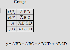
 Using the Boolean logic expression below, draw circuit diagram with logic gates that will implement your Boolean expression without simplifying or expanding the expression. F(A, B, C, D) = ABD + ABCD + ABCD + ABCD Complete a Truth Table F(A, B, C, D). Use your logic circuit diagram and Boolean logic expression as much as possible.
4. Implement the function using only NOR gates (20 pts) (A B+C).D Sketch the logic gate...
 4. Implement the function using only NOR gates (20 pts) (A B+C).D Sketch the logic gate schematic and verify your circuit by truth table.
Q. Implement [F = (A+B+C).(D+E) ] using Static CMOS logic, transmission gates and pass transistors. "This is...
Q. Implement [F = (A+B+C).(D+E) ] using Static CMOS logic, transmission gates and pass transistors. "This is a question of CMOS VLSI Design "
Class 24 1. Given the shorthand POS expression F(a,b,c,d) П M (0,6,7,8) (b + c + d)(a + D+ ē): a....
 Class 24 1. Given the shorthand POS expression F(a,b,c,d) П M (0,6,7,8) (b + c + d)(a + D+ ē): a. (25 points) Implement F using one 4-to-16 decoder and one OR gate of any size. b. (25 points) Implement F using four 2-40-4 decoders and one OR gate of any size. c. (25 points) Implement F using just two 8-to-3 encoders, NOT gates, and one AND gate of any size. Hint: given NOT gates and an AND gate to...
Use only 2-to-1 multiplexers to implement the circuit for the following function: F(A, B, C) =...
 Use only 2-to-1 multiplexers to implement the circuit for the following function: F(A, B, C) = Pi M (1, 2, 4, 5) Assume the inverse of each input variable is available, (i.e., you can directly use the inverse of each input variable A, B, or C, in your answer.) Repeat P7, but this time using only one 4-to-1 multiplexer.
Design the circuit for f(A,B,C,D)=ΠM(0,1,4,7,8,12-15),d(2,3,10) using a minimal number of 3-to-8 line decoders and NAND gates...
Design the circuit for f(A,B,C,D)=ΠM(0,1,4,7,8,12-15),d(2,3,10) using a minimal number of 3-to-8 line decoders and NAND gates (any size). Decoder outputs must be active-low. Also, assume that the decoder has one active-high enable line G0. If you need NOT gates, you must show them in the diagram using NAND gates.
There are two multiplexers in the following circuit. The three ports A, B, C are inputs,...
 There are two multiplexers in the following circuit. The three ports A, B, C are inputs, and s) uput(1) Write a truth table for the logic function Y F(A, B, C) of the following cirouit (2) ne inimized Boolean equation for the logic function. B C 01 10 ground P. (5 pts). Use a decoder to implement the following Boolean logic function: Y= AB+AC. Draw schematic of your circuit.
1. Q(A,B,C,D) = ABC'+ A'BC+C'D'+AB'+B'C a) Implement the previous function using logic gates. b) implement the...
1. Q(A,B,C,D) = ABC'+ A'BC+C'D'+AB'+B'C a) Implement the previous function using logic gates. b) implement the same function using a 16 input multiplexer (74150) only. (Hint: draw the truth table for Q)
 Implement the circuit defined by equation F(a,b,c,d) = ∑( )
using:
a. -to- multiplexers and logic gates.
b. -to- decoders and logic gates.
(0,5,6,7,11) 3. Implement the circuit defined by equation F(a,b,c,d) = using: a. 4-to-1 multiplexers and logic gates. b. 2-to-4 decoders and logic gates.
Implement the circuit defined by equation F(a,b,c,d) = ∑( )
using:
a. -to- multiplexers and logic gates.
b. -to- decoders and logic gates.
(0,5,6,7,11) 3. Implement the circuit defined by equation F(a,b,c,d) = using: a. 4-to-1 multiplexers and logic gates. b. 2-to-4 decoders and logic gates.
 Using the Boolean logic expression below, draw circuit diagram with logic gates that will implement your Boolean expression without simplifying or expanding the expression. F(A, B, C, D) = ABD + ABCD + ABCD + ABCD Complete a Truth Table F(A, B, C, D). Use your logic circuit diagram and Boolean logic expression as much as possible.
 4. Implement the function using only NOR gates (20 pts) (A B+C).D Sketch the logic gate schematic and verify your circuit by truth table.
 Class 24 1. Given the shorthand POS expression F(a,b,c,d) П M (0,6,7,8) (b + c + d)(a + D+ ē): a. (25 points) Implement F using one 4-to-16 decoder and one OR gate of any size. b. (25 points) Implement F using four 2-40-4 decoders and one OR gate of any size. c. (25 points) Implement F using just two 8-to-3 encoders, NOT gates, and one AND gate of any size. Hint: given NOT gates and an AND gate to...
 Use only 2-to-1 multiplexers to implement the circuit for the following function: F(A, B, C) = Pi M (1, 2, 4, 5) Assume the inverse of each input variable is available, (i.e., you can directly use the inverse of each input variable A, B, or C, in your answer.) Repeat P7, but this time using only one 4-to-1 multiplexer.
 There are two multiplexers in the following circuit. The three ports A, B, C are inputs, and s) uput(1) Write a truth table for the logic function Y F(A, B, C) of the following cirouit (2) ne inimized Boolean equation for the logic function. B C 01 10 ground P. (5 pts). Use a decoder to implement the following Boolean logic function: Y= AB+AC. Draw schematic of your circuit.
Most questions answered within 3 hours.
-
For a class science experiment, the students had to grow beans
in a cup and see...
asked 2 minutes ago -
CASE STUDY
The phrase ‘OK Boomer’ has gone viral recently as a way to
shut down...
asked 15 minutes ago -
The following thermochemical equation is for the reaction of
nitrogen(g) with oxygen(g) to form nitrogen dioxide(g)....
asked 11 minutes ago -
the solubility of an unknown salt M3Z2 at 25 degrees is
4.9*10^-7 mol/L. what is the...
asked 12 minutes ago -
We would like to create an Assembly program whose executable is
called division.exe and that behaves...
asked 13 minutes ago -
Consider a simple paging system with the following parameters:
232 bytes of physical memory; page size...
asked 14 minutes ago -
a raindrop of mass 2.00 g falls on the roof of a car with an
initial...
asked 36 minutes ago -
An environmental economic consulting firm is hired to measure
the negative externalities associated with the pollution...
asked 36 minutes ago -
Express Catering contributed $8,000 to the American Lung
Association. If taxable income, before charitable contribution is...
asked 28 minutes ago -
Why we should not allow the Oil & Gas industry to
explore, exploit and extract oil...
asked 39 minutes ago -
In the readings for this topic, the methods for gathering data are
provided. However, there is...
asked 51 minutes ago -
Select from the option list provided the most likely
classification(s) of net assets, if any, that...
asked 51 minutes ago