
Homework Answers
We found this as -


Add Answer to:
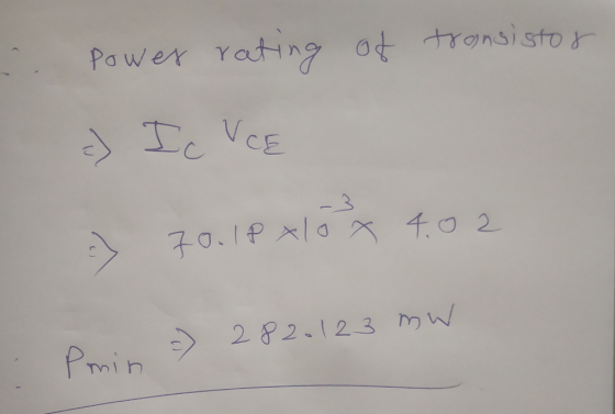
ee e A Quèstion 27 Calculate the minimum power rating (Po) for transistor in the loaded Common Emitter Amplifier be...
Blackboard X A wOVIny T0anoer queauoTWaaveUnT0aUrie Question 24 Calculate the power gain (Ap) for the loaded Common...
 Blackboard X A wOVIny T0anoer queauoTWaaveUnT0aUrie Question 24 Calculate the power gain (Ap) for the loaded Common Emitter Amplifier below Assume BAC200, Assume re' 16 0 Vcc 15 V R1 66.4 KQ, R2 25.8 KO Rc 3.9 KQ RE1 3300, RE2 1.8 KO, RL 3.54 KO Enter your results. No units. SR1 RC C3 Vcc Vout Vin HH Beta RL Vs R2 RE1 RE2 C2 AMoving to another question will save this response. ww
Blackboard X A wOVIny T0anoer queauoTWaaveUnT0aUrie...
Blackboard X A wOVIny T0anoer queauoTWaaveUnT0aUrie Question 24 Calculate the power gain (Ap) for the loaded Common Emitter Amplifier below Assume BAC200, Assume re' 16 0 Vcc 15 V R1 66.4 KQ, R2 25.8 KO Rc 3.9 KQ RE1 3300, RE2 1.8 KO, RL 3.54 KO Enter your results. No units. SR1 RC C3 Vcc Vout Vin HH Beta RL Vs R2 RE1 RE2 C2 AMoving to another question will save this response. ww
Blackboard X A wOVIny T0anoer queauoTWaaveUnT0aUrie...
Question 26 Calculate the output power Pout (RL) for the unloaded Common Emitter Amplifier below BDC=200, BAC =...
 Question 26 Calculate the output power Pout (RL) for the unloaded Common Emitter Amplifier below BDC=200, BAC = 150, re 0.39 Vs- 538 mVpp, Vcc 15 V, R1=1 KQ, R2 = 330 2 RC= 1000, RE1= 8.20, RE2= 36 0, RL 0.19 KO Enter your results in mW. SR1 RL Vcc C1 Vin Beta Vs R2 RE1 RE2 C2 ww
Question 26 Calculate the output power Pout (RL) for the unloaded Common Emitter Amplifier below BDC=200, BAC = 150, re...
Question 26 Calculate the output power Pout (RL) for the unloaded Common Emitter Amplifier below BDC=200, BAC = 150, re 0.39 Vs- 538 mVpp, Vcc 15 V, R1=1 KQ, R2 = 330 2 RC= 1000, RE1= 8.20, RE2= 36 0, RL 0.19 KO Enter your results in mW. SR1 RL Vcc C1 Vin Beta Vs R2 RE1 RE2 C2 ww
Question 26 Calculate the output power Pout (RL) for the unloaded Common Emitter Amplifier below BDC=200, BAC = 150, re...
Calculate the voltage gain (Av) for the loaded Common Emitter Amplifier below: BAC 200 for all...
 Calculate the voltage gain (Av) for the loaded Common Emitter Amplifier below: BAC 200 for all transistors. Assume re 15 Q for the CE Amplifier. Ignore re' for the DP Amplifier Vcc 12 V, R1 56 K, R2 10 KQ, R4 22 KQ R3 5.6 KQ, RL 8 RE(CE) 628 0, RE(CC) 330 Rc 3.5 KQ, Enter your results. No units. SR3 R1 RC C3 Vcc C1 Beta Q2a HH Vin Beta Q1 Beta Q2b C4 R4 Vs R2 C2...
Calculate the power gain (Ap) for the loaded Common Collecter Amplifier below: Assume Av1, BAC-180, lanore...
 Calculate the power gain (Ap) for the loaded Common Collecter Amplifier below: Assume Av1, BAC-180, lanore re Vec-15 V R1=39 KO R2-220 KQ RE=1 KO. RL-0.8 KQ Enter your results. No units. Vcc C1 Beta Vout RL RE
Calculate the power consumption from the DC power supply for our two transistor amplifier when there...
 Calculate the power consumption from the DC power supply for our
two transistor amplifier when there is no AC input signal.
R1 47k RC 2.74k Vout Cin Vin 220n RS 470 47micro 2N3904 8 Ohm SPKR R2 10k RE 1k RE' 820 5 1 47micro Common Emitter Stage Emitter Follower Stage
Calculate the power consumption from the DC power supply for our
two transistor amplifier when there is no AC input signal.
R1 47k RC 2.74k Vout Cin Vin 220n RS 470 47micro 2N3904 8 Ohm SPKR R2 10k RE 1k RE' 820 5 1 47micro Common Emitter Stage Emitter Follower Stage
please I need details l and....Debate Club | Offic A) Theoretical Design Design a common emitter BJT amplifier with the following requirements: -Rin-10 K2, and Ro-45 ㏀ (Neglect the Early voltage...
 please I need details
l and....Debate Club | Offic A) Theoretical Design Design a common emitter BJT amplifier with the following requirements: -Rin-10 K2, and Ro-45 ㏀ (Neglect the Early voltage Effect) Vo/Vsig- Gv-40 VIV or 32 dB " VCC-9 V V, IC-1mA, VCE-3.25V and β-100 RL-40 kQ, Rsige I ka, R 1-3R2, and C1-C2-1 μF Voc RC C2 R1 Rsig C1 RL R2 RE B) Verify your design using Orcad Capture Pspice by doing 1) AC sweep (frequency response):...
please I need details
l and....Debate Club | Offic A) Theoretical Design Design a common emitter BJT amplifier with the following requirements: -Rin-10 K2, and Ro-45 ㏀ (Neglect the Early voltage Effect) Vo/Vsig- Gv-40 VIV or 32 dB " VCC-9 V V, IC-1mA, VCE-3.25V and β-100 RL-40 kQ, Rsige I ka, R 1-3R2, and C1-C2-1 μF Voc RC C2 R1 Rsig C1 RL R2 RE B) Verify your design using Orcad Capture Pspice by doing 1) AC sweep (frequency response):...
F LOpoint For the circuit shown in Figure 3 3. 1. Draw the DC equivalent circuit...
 F LOpoint For the circuit shown in Figure 3 3. 1. Draw the DC equivalent circuit by opening caps and shorting inductors 2. Analyze the DC equivalent circuit as we have in previous labs (assume a region, analyze and check assumptions). Check your DC operating point using LT Spice. 3. Calculate the small signal parameters (transconductance, output resistance, input resistance) 4. Draw the AC equivalent circuit by shorting de voltage sources, opening dc current sources, shorting caps and opening inductors....
 Blackboard X A wOVIny T0anoer queauoTWaaveUnT0aUrie Question 24 Calculate the power gain (Ap) for the loaded Common Emitter Amplifier below Assume BAC200, Assume re' 16 0 Vcc 15 V R1 66.4 KQ, R2 25.8 KO Rc 3.9 KQ RE1 3300, RE2 1.8 KO, RL 3.54 KO Enter your results. No units. SR1 RC C3 Vcc Vout Vin HH Beta RL Vs R2 RE1 RE2 C2 AMoving to another question will save this response. ww
Blackboard X A wOVIny T0anoer queauoTWaaveUnT0aUrie...
Blackboard X A wOVIny T0anoer queauoTWaaveUnT0aUrie Question 24 Calculate the power gain (Ap) for the loaded Common Emitter Amplifier below Assume BAC200, Assume re' 16 0 Vcc 15 V R1 66.4 KQ, R2 25.8 KO Rc 3.9 KQ RE1 3300, RE2 1.8 KO, RL 3.54 KO Enter your results. No units. SR1 RC C3 Vcc Vout Vin HH Beta RL Vs R2 RE1 RE2 C2 AMoving to another question will save this response. ww
Blackboard X A wOVIny T0anoer queauoTWaaveUnT0aUrie...
 Question 26 Calculate the output power Pout (RL) for the unloaded Common Emitter Amplifier below BDC=200, BAC = 150, re 0.39 Vs- 538 mVpp, Vcc 15 V, R1=1 KQ, R2 = 330 2 RC= 1000, RE1= 8.20, RE2= 36 0, RL 0.19 KO Enter your results in mW. SR1 RL Vcc C1 Vin Beta Vs R2 RE1 RE2 C2 ww
Question 26 Calculate the output power Pout (RL) for the unloaded Common Emitter Amplifier below BDC=200, BAC = 150, re...
Question 26 Calculate the output power Pout (RL) for the unloaded Common Emitter Amplifier below BDC=200, BAC = 150, re 0.39 Vs- 538 mVpp, Vcc 15 V, R1=1 KQ, R2 = 330 2 RC= 1000, RE1= 8.20, RE2= 36 0, RL 0.19 KO Enter your results in mW. SR1 RL Vcc C1 Vin Beta Vs R2 RE1 RE2 C2 ww
Question 26 Calculate the output power Pout (RL) for the unloaded Common Emitter Amplifier below BDC=200, BAC = 150, re...
 Calculate the voltage gain (Av) for the loaded Common Emitter Amplifier below: BAC 200 for all transistors. Assume re 15 Q for the CE Amplifier. Ignore re' for the DP Amplifier Vcc 12 V, R1 56 K, R2 10 KQ, R4 22 KQ R3 5.6 KQ, RL 8 RE(CE) 628 0, RE(CC) 330 Rc 3.5 KQ, Enter your results. No units. SR3 R1 RC C3 Vcc C1 Beta Q2a HH Vin Beta Q1 Beta Q2b C4 R4 Vs R2 C2...
 Calculate the power gain (Ap) for the loaded Common Collecter Amplifier below: Assume Av1, BAC-180, lanore re Vec-15 V R1=39 KO R2-220 KQ RE=1 KO. RL-0.8 KQ Enter your results. No units. Vcc C1 Beta Vout RL RE
 Calculate the power consumption from the DC power supply for our
two transistor amplifier when there is no AC input signal.
R1 47k RC 2.74k Vout Cin Vin 220n RS 470 47micro 2N3904 8 Ohm SPKR R2 10k RE 1k RE' 820 5 1 47micro Common Emitter Stage Emitter Follower Stage
Calculate the power consumption from the DC power supply for our
two transistor amplifier when there is no AC input signal.
R1 47k RC 2.74k Vout Cin Vin 220n RS 470 47micro 2N3904 8 Ohm SPKR R2 10k RE 1k RE' 820 5 1 47micro Common Emitter Stage Emitter Follower Stage
 please I need details
l and....Debate Club | Offic A) Theoretical Design Design a common emitter BJT amplifier with the following requirements: -Rin-10 K2, and Ro-45 ㏀ (Neglect the Early voltage Effect) Vo/Vsig- Gv-40 VIV or 32 dB " VCC-9 V V, IC-1mA, VCE-3.25V and β-100 RL-40 kQ, Rsige I ka, R 1-3R2, and C1-C2-1 μF Voc RC C2 R1 Rsig C1 RL R2 RE B) Verify your design using Orcad Capture Pspice by doing 1) AC sweep (frequency response):...
please I need details
l and....Debate Club | Offic A) Theoretical Design Design a common emitter BJT amplifier with the following requirements: -Rin-10 K2, and Ro-45 ㏀ (Neglect the Early voltage Effect) Vo/Vsig- Gv-40 VIV or 32 dB " VCC-9 V V, IC-1mA, VCE-3.25V and β-100 RL-40 kQ, Rsige I ka, R 1-3R2, and C1-C2-1 μF Voc RC C2 R1 Rsig C1 RL R2 RE B) Verify your design using Orcad Capture Pspice by doing 1) AC sweep (frequency response):...
 F LOpoint For the circuit shown in Figure 3 3. 1. Draw the DC equivalent circuit by opening caps and shorting inductors 2. Analyze the DC equivalent circuit as we have in previous labs (assume a region, analyze and check assumptions). Check your DC operating point using LT Spice. 3. Calculate the small signal parameters (transconductance, output resistance, input resistance) 4. Draw the AC equivalent circuit by shorting de voltage sources, opening dc current sources, shorting caps and opening inductors....
Most questions answered within 3 hours.
-
3) What are the typical social structures in a global city?
asked 1 hour ago -
Luther Corporation
Consolidated Balance Sheet
December 31, 2019 and 2018 (in $ millions)
Assets
2019
2018...
asked 1 hour ago -
(Expected rate of return and risk) Carter Inc. is evaluating a
security. Calculate the investment’s expected...
asked 3 hours ago -
What specific indicators can point to lack of progress for
African Americans in American society?
asked 4 hours ago -
1-The Electrons in a beam are moving at 2.7×10⁸ m/s in an
electric field of 15000...
asked 5 hours ago -
A gas tank is a vertical cylinder. It has a radius of 1m, a
height of...
asked 5 hours ago -
Accent Software faces the following conditions. All of these
support Accent’s use of a market-penetration pricing...
asked 6 hours ago -
A mathematically inclined friend emails you the following
instructions: "Meet me in the cafeteria the first...
asked 6 hours ago -
A monopoly sells in two countries . The demand curves in the two
countries are p1...
asked 7 hours ago -
A .15kg rubber ball is bounced off a wall. Before hitting the
wall, the ball moves...
asked 8 hours ago -
A manufacturing company preparing to build a new plant is
considering three potential locations for it....
asked 8 hours ago -
B. If compound Y has approximately the same values of solubility
in toluene as compound X,...
asked 9 hours ago