
Homework Answers


Add Answer to:
please answer this ASAP Answer the following questions for the below BJT amplifier circuit. Assume capacitors...
The BJT amplifier circuit in the figure below has β = 90. Use VT = 25...
 The BJT amplifier circuit in the figure below has β = 90. Use VT
= 25 mV
a- Draw the DC equivalent circuit and calculate IC.
b- Draw the small signal equivalent circuit and calculate the
small signal parameters.
c- Find the voltage gain
+9V 3 kΩ C2 = 1 uF HE C = 1uF + υο 10 kΩ Cz = 50 uF - . υ 9 kΩ Η. 6. ΚΩ -9 V
The BJT amplifier circuit in the figure below has β = 90. Use VT
= 25 mV
a- Draw the DC equivalent circuit and calculate IC.
b- Draw the small signal equivalent circuit and calculate the
small signal parameters.
c- Find the voltage gain
+9V 3 kΩ C2 = 1 uF HE C = 1uF + υο 10 kΩ Cz = 50 uF - . υ 9 kΩ Η. 6. ΚΩ -9 V
1. Consider the Common-Emitter BJT amplifier circuit, shown below. VD VOD BJT Parameters: B=99 A/A i=0...
 1. Consider the Common-Emitter BJT amplifier circuit, shown below. VD VOD BJT Parameters: B=99 A/A i=0 RE Co Circuit Parameters: Ca Cc2 = 0 F Car = OF R = 2022 R = 2002 R1 = 25.8 k22 Ry2 = 51.6 ks V = 15 V VEE=0 V Сct Active Mode: Va >0.2 V Vwx=0.7V Ic=B1, Ic=al, 1 R2 3 SRCA a) Find the open-circuit voltage gain, Ave, of this amplifier circuit. Verify your assumptions. b) Compute the input resistance,...
Problem 2: Consider the following amplifier circuit. All capacitors are infinite valued. Voc RB1 Rc1 Rc2...
 Problem 2: Consider the following amplifier circuit. All capacitors are infinite valued. Voc RB1 Rc1 Rc2 0 Q1 Vout RB2 Rout1 Q2 Rout2 Rint R1 Rin2 Rsig + IEI Vsig Voc SINE() IE2 a. Specify the type of amplifier in each stage. b. Draw the small signal model of this amplifier and include the early effect. c. Derive an expression for Rout1 and Rout2 including early effect. d. Derive expressions for Rin1 and Rin2. Ignore the early effect. e. Derive...
Rsig Nahyan vgs ( gmugs, r01 RDS Vsig ) Ril Consider the small signal equivalent circuit...
 Rsig Nahyan vgs ( gmugs, r01 RDS Vsig ) Ril Consider the small signal equivalent circuit of an amplifier shown above. The parameters are given to be: R1 = 3000, R2 = 10160, R2=100%, RD=RL=50 Rsig = 202, VGS1=3.5V. Vt = 0.5V and kn = 1mA/V^2. The transistor output resistances are represented by ro1, ra2 with both the transistors in saturation and having |MAL= 40V and same DC current flowing through them Find the small signal parameter of the MOSFET:...
Please show steps & explain. WILL RATE!!! 7.133 For the circuit below, find the input resistance...
 Please show steps &
explain. WILL RATE!!!
7.133 For the circuit below, find the input resistance Rin and the voltage gain v./Vsig. Assume that the source provides a small signal Vsig and that ß = 100. 0.5 mA tovo § 5 KN 100 kN 3 Rsig = 50 12 U18
Please show steps &
explain. WILL RATE!!!
7.133 For the circuit below, find the input resistance Rin and the voltage gain v./Vsig. Assume that the source provides a small signal Vsig and that ß = 100. 0.5 mA tovo § 5 KN 100 kN 3 Rsig = 50 12 U18
6.5 BI C2 Cl sig in 0 Design the bias circuit of the CE amplifier shown...
 6.5 BI C2 Cl sig in 0 Design the bias circuit of the CE amplifier shown to obtain IE= 0.5 mA and Vc= +6 V. Design for a dc voltage at the base of 5 V and a current through RB2 of 50 μΑ. Let Vcc-+15 V, β-100, and VBE 0.7 V. a) Specify the values of RBi, RB2, RE, and Rc b) Also give the values of the BJT small-signal parameters gm, rr , and ro at the bias...
Q1. For the cascade amplifier circuit shown in Fig (1): a) What are the functions of the capacitors C, C2 and C3? And w...
 Q1. For the cascade amplifier circuit shown in Fig (1): a) What are the functions of the capacitors C, C2 and C3? And what are the functions of the capacitors Cs and CE? b) What are the functions of the resistors RD and Rc? c) Draw the DC biasing circuits for each stage. d) Find loa, VGsa, VDs and gm for the JFET stage (you may use either mathematical or graphical methods) e) Calculate l, Ic, le and Ve for...
7.53 For the circuit shown in Fig. P7.53, draw a complete small-signal equivalent circuit utilizing an...
 7.53 For the circuit shown in Fig. P7.53, draw a complete small-signal equivalent circuit utilizing an appropriate T model for the BJT (use a =0.99). Your circuit should show the values of all components, including the model parameters. What is the input resistance R ? Calculate the overall voltage gain (v,/v). (also find A, for this amp) sig +5 V RC 12 kΩ C2 RL 12 ΚΩ Rsig 75 N ) 0.33 mA Vsig Rin Figure P7.53
11.41 O The circuit of Fig. P11.41 represents the inter- nal circuitry of a simple BJT...
 11.41 O The circuit of Fig. P11.41 represents the inter- nal circuitry of a simple BJT operational amplifier. In answering the following questions, use appropriate en- gineering approximations where required. Assume the BJTs in the circuit to be matched and to have the fol- lowing parameters: Cli = 1 pF, VA 00, VBE = 0.7 V, Vsat 0.2 V,尾= 200, and η = 1 . Find the bias currents through each BJT and the bias voltages of nodes A, B,...
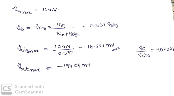
Vsig = 10mV*sin(2Kπ) The circuit above is a common-emitter amplifier. Given the parameters in the circuit,...
 Vsig = 10mV*sin(2Kπ)
The circuit above is a common-emitter amplifier. Given the
parameters in the circuit,
1. If Rb1=10KΩ, Calculate Rb2, Ib, Ic, Ie, Re, transconductance
(gm), Current through Rb1 (I_rb1), and Current through Rb2(I_rb2),
Vb, Vc, Ve, Vce. Also, calculate Rc to achieve a voltage gain Av =
- 100 V/
(If Rb1 value does not match up, then choose your resistor
value for Rb1.)
2. If the amplitude of Vsig keeps increasing, at what amplitude
of the input...
Vsig = 10mV*sin(2Kπ)
The circuit above is a common-emitter amplifier. Given the
parameters in the circuit,
1. If Rb1=10KΩ, Calculate Rb2, Ib, Ic, Ie, Re, transconductance
(gm), Current through Rb1 (I_rb1), and Current through Rb2(I_rb2),
Vb, Vc, Ve, Vce. Also, calculate Rc to achieve a voltage gain Av =
- 100 V/
(If Rb1 value does not match up, then choose your resistor
value for Rb1.)
2. If the amplitude of Vsig keeps increasing, at what amplitude
of the input...
 The BJT amplifier circuit in the figure below has β = 90. Use VT
= 25 mV
a- Draw the DC equivalent circuit and calculate IC.
b- Draw the small signal equivalent circuit and calculate the
small signal parameters.
c- Find the voltage gain
+9V 3 kΩ C2 = 1 uF HE C = 1uF + υο 10 kΩ Cz = 50 uF - . υ 9 kΩ Η. 6. ΚΩ -9 V
The BJT amplifier circuit in the figure below has β = 90. Use VT
= 25 mV
a- Draw the DC equivalent circuit and calculate IC.
b- Draw the small signal equivalent circuit and calculate the
small signal parameters.
c- Find the voltage gain
+9V 3 kΩ C2 = 1 uF HE C = 1uF + υο 10 kΩ Cz = 50 uF - . υ 9 kΩ Η. 6. ΚΩ -9 V
 1. Consider the Common-Emitter BJT amplifier circuit, shown below. VD VOD BJT Parameters: B=99 A/A i=0 RE Co Circuit Parameters: Ca Cc2 = 0 F Car = OF R = 2022 R = 2002 R1 = 25.8 k22 Ry2 = 51.6 ks V = 15 V VEE=0 V Сct Active Mode: Va >0.2 V Vwx=0.7V Ic=B1, Ic=al, 1 R2 3 SRCA a) Find the open-circuit voltage gain, Ave, of this amplifier circuit. Verify your assumptions. b) Compute the input resistance,...
 Problem 2: Consider the following amplifier circuit. All capacitors are infinite valued. Voc RB1 Rc1 Rc2 0 Q1 Vout RB2 Rout1 Q2 Rout2 Rint R1 Rin2 Rsig + IEI Vsig Voc SINE() IE2 a. Specify the type of amplifier in each stage. b. Draw the small signal model of this amplifier and include the early effect. c. Derive an expression for Rout1 and Rout2 including early effect. d. Derive expressions for Rin1 and Rin2. Ignore the early effect. e. Derive...
 Rsig Nahyan vgs ( gmugs, r01 RDS Vsig ) Ril Consider the small signal equivalent circuit of an amplifier shown above. The parameters are given to be: R1 = 3000, R2 = 10160, R2=100%, RD=RL=50 Rsig = 202, VGS1=3.5V. Vt = 0.5V and kn = 1mA/V^2. The transistor output resistances are represented by ro1, ra2 with both the transistors in saturation and having |MAL= 40V and same DC current flowing through them Find the small signal parameter of the MOSFET:...
 Please show steps &
explain. WILL RATE!!!
7.133 For the circuit below, find the input resistance Rin and the voltage gain v./Vsig. Assume that the source provides a small signal Vsig and that ß = 100. 0.5 mA tovo § 5 KN 100 kN 3 Rsig = 50 12 U18
Please show steps &
explain. WILL RATE!!!
7.133 For the circuit below, find the input resistance Rin and the voltage gain v./Vsig. Assume that the source provides a small signal Vsig and that ß = 100. 0.5 mA tovo § 5 KN 100 kN 3 Rsig = 50 12 U18
 6.5 BI C2 Cl sig in 0 Design the bias circuit of the CE amplifier shown to obtain IE= 0.5 mA and Vc= +6 V. Design for a dc voltage at the base of 5 V and a current through RB2 of 50 μΑ. Let Vcc-+15 V, β-100, and VBE 0.7 V. a) Specify the values of RBi, RB2, RE, and Rc b) Also give the values of the BJT small-signal parameters gm, rr , and ro at the bias...
 Q1. For the cascade amplifier circuit shown in Fig (1): a) What are the functions of the capacitors C, C2 and C3? And what are the functions of the capacitors Cs and CE? b) What are the functions of the resistors RD and Rc? c) Draw the DC biasing circuits for each stage. d) Find loa, VGsa, VDs and gm for the JFET stage (you may use either mathematical or graphical methods) e) Calculate l, Ic, le and Ve for...
 7.53 For the circuit shown in Fig. P7.53, draw a complete small-signal equivalent circuit utilizing an appropriate T model for the BJT (use a =0.99). Your circuit should show the values of all components, including the model parameters. What is the input resistance R ? Calculate the overall voltage gain (v,/v). (also find A, for this amp) sig +5 V RC 12 kΩ C2 RL 12 ΚΩ Rsig 75 N ) 0.33 mA Vsig Rin Figure P7.53
 11.41 O The circuit of Fig. P11.41 represents the inter- nal circuitry of a simple BJT operational amplifier. In answering the following questions, use appropriate en- gineering approximations where required. Assume the BJTs in the circuit to be matched and to have the fol- lowing parameters: Cli = 1 pF, VA 00, VBE = 0.7 V, Vsat 0.2 V,尾= 200, and η = 1 . Find the bias currents through each BJT and the bias voltages of nodes A, B,...
 Vsig = 10mV*sin(2Kπ)
The circuit above is a common-emitter amplifier. Given the
parameters in the circuit,
1. If Rb1=10KΩ, Calculate Rb2, Ib, Ic, Ie, Re, transconductance
(gm), Current through Rb1 (I_rb1), and Current through Rb2(I_rb2),
Vb, Vc, Ve, Vce. Also, calculate Rc to achieve a voltage gain Av =
- 100 V/
(If Rb1 value does not match up, then choose your resistor
value for Rb1.)
2. If the amplitude of Vsig keeps increasing, at what amplitude
of the input...
Vsig = 10mV*sin(2Kπ)
The circuit above is a common-emitter amplifier. Given the
parameters in the circuit,
1. If Rb1=10KΩ, Calculate Rb2, Ib, Ic, Ie, Re, transconductance
(gm), Current through Rb1 (I_rb1), and Current through Rb2(I_rb2),
Vb, Vc, Ve, Vce. Also, calculate Rc to achieve a voltage gain Av =
- 100 V/
(If Rb1 value does not match up, then choose your resistor
value for Rb1.)
2. If the amplitude of Vsig keeps increasing, at what amplitude
of the input...
Most questions answered within 3 hours.
-
(Expected rate of return and risk) Carter Inc. is evaluating a
security. Calculate the investment’s expected...
asked 2 hours ago -
What specific indicators can point to lack of progress for
African Americans in American society?
asked 3 hours ago -
1-The Electrons in a beam are moving at 2.7×10⁸ m/s in an
electric field of 15000...
asked 3 hours ago -
A gas tank is a vertical cylinder. It has a radius of 1m, a
height of...
asked 3 hours ago -
Accent Software faces the following conditions. All of these
support Accent’s use of a market-penetration pricing...
asked 4 hours ago -
A mathematically inclined friend emails you the following
instructions: "Meet me in the cafeteria the first...
asked 4 hours ago -
A monopoly sells in two countries . The demand curves in the two
countries are p1...
asked 5 hours ago -
A .15kg rubber ball is bounced off a wall. Before hitting the
wall, the ball moves...
asked 6 hours ago -
A manufacturing company preparing to build a new plant is
considering three potential locations for it....
asked 6 hours ago -
B. If compound Y has approximately the same values of solubility
in toluene as compound X,...
asked 7 hours ago -
Oscar Inc. has inventory in Japan valued at 39,051,000 Yen one
year ago. One year ago...
asked 7 hours ago -
If Canada suffered from "fundamental disequilibrium," and its
government choose not to devalue its currency, a...
asked 7 hours ago