
Homework Answers
Add Answer to:
7.53 For the circuit shown in Fig. P7.53, draw a complete small-signal equivalent circuit utilizing an...
6.5 BI C2 Cl sig in 0 Design the bias circuit of the CE amplifier shown...
 6.5 BI C2 Cl sig in 0 Design the bias circuit of the CE amplifier shown to obtain IE= 0.5 mA and Vc= +6 V. Design for a dc voltage at the base of 5 V and a current through RB2 of 50 μΑ. Let Vcc-+15 V, β-100, and VBE 0.7 V. a) Specify the values of RBi, RB2, RE, and Rc b) Also give the values of the BJT small-signal parameters gm, rr , and ro at the bias...
it of Fig. P6.120, the BJT is biased with nt source, and vsig is a small...
 it of Fig. P6.120, the BJT is biased with nt source, and vsig is a small sine-wave signal. Fi 6.120 In the circuit +3 V 20 kΩ 20 kΩ 20 kΩ 200 kΩ 0.1 mA Rin Figure P6.120 Find Rin and the gain terag. Assume β 100. If the amplitude of the signal Vbe is to be limited to 5 mV, what is the largest signal at the input? What is the corresponding signal at the output? sig
Rsig Nahyan vgs ( gmugs, r01 RDS Vsig ) Ril Consider the small signal equivalent circuit...
 Rsig Nahyan vgs ( gmugs, r01 RDS Vsig ) Ril Consider the small signal equivalent circuit of an amplifier shown above. The parameters are given to be: R1 = 3000, R2 = 10160, R2=100%, RD=RL=50 Rsig = 202, VGS1=3.5V. Vt = 0.5V and kn = 1mA/V^2. The transistor output resistances are represented by ro1, ra2 with both the transistors in saturation and having |MAL= 40V and same DC current flowing through them Find the small signal parameter of the MOSFET:...
Q. 4. (a) Draw a small signal equivalent circuit by replacing the BJT with its hybrid-mt...
 Q. 4. (a) Draw a small signal equivalent circuit by replacing the BJT with its hybrid-mt model for the circuit shown below. Also derive an expression for Zin when la is neglected. (10) + Vx (b) Compute the voltage gain, input and output impedance for the following circuit if ß = 150 and VBEQ = 0.7 V, V1 = 26 mV. (15) A+ 10 V 40 ΚΩ R1 4 ΚΩ Сі CO Vs R2 vo 60 ΚΩ 5 ΚΩ RE...
Design the CS amplifier in Fig. L7.17(a) to achieve a small-signal gain of at least 4,--5 V/V. Us...
 Design the CS amplifier in Fig. L7.17(a) to achieve a small-signal gain of at least 4,--5 V/V. Use supplies of V+--K = 15 V, Rsig-50 Ω, RL-10 kQ, and R1R2 = 10 kQ, and design the circuit to have ID-1 mA and a DC voltage at the gate Vo = 0 V. Use Cc,-CC2-CS-47 μF. What is the expected DC voltage at the source of the NMOS? C1 sig V. Rs sig
Design the CS amplifier in Fig. L7.17(a) to...
Design the CS amplifier in Fig. L7.17(a) to achieve a small-signal gain of at least 4,--5 V/V. Use supplies of V+--K = 15 V, Rsig-50 Ω, RL-10 kQ, and R1R2 = 10 kQ, and design the circuit to have ID-1 mA and a DC voltage at the gate Vo = 0 V. Use Cc,-CC2-CS-47 μF. What is the expected DC voltage at the source of the NMOS? C1 sig V. Rs sig
Design the CS amplifier in Fig. L7.17(a) to...
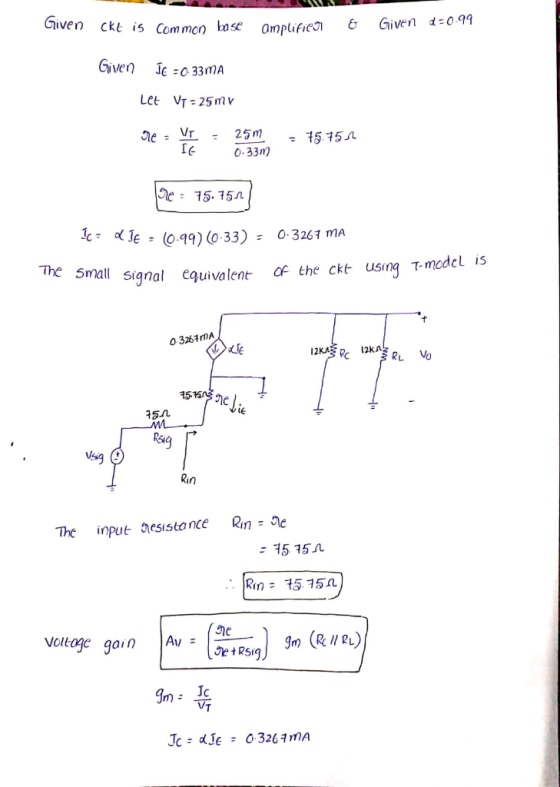
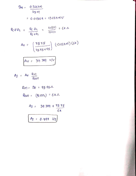
The given BJT has α =0.99 1- Use P spice to simulate the given circuit, then...
 The given BJT has α =0.99
1- Use P spice to simulate the given circuit, then find the
values of the base, collector and emitter currents.
2- Calculate theoretically the three terminals ‘currents.
3- Use T-model to draw the small-signal equivalent circuit.
4- Calculate the input resistance.
5- Calculate the overall gain.
can any one answer the questions today please ?
+9V 10 k12 C2 0. 8 21 Rz 10 k12 Rsig C 50 12 00 Usig 0.5 mA +...
The given BJT has α =0.99
1- Use P spice to simulate the given circuit, then find the
values of the base, collector and emitter currents.
2- Calculate theoretically the three terminals ‘currents.
3- Use T-model to draw the small-signal equivalent circuit.
4- Calculate the input resistance.
5- Calculate the overall gain.
can any one answer the questions today please ?
+9V 10 k12 C2 0. 8 21 Rz 10 k12 Rsig C 50 12 00 Usig 0.5 mA +...
In the circuit of given below, Vsig is a small sine wave signal with zero average. The transistor...
 In the circuit of given below, Vsig is a small sine wave signal with zero average. The transistor B is 100. a) Find the value of RE to establish a dc emitter current of about 0.5 mA. b) Find Rc to establish a dc collector voltage of about +5 V c) For RL10 kS2 and the transistor ro 200 k2, draw the small-signal equivalent circuit 5. of the amplifier and determine its overall voltage gain +15 V Re O Vo...
Q.A. 2 -Statement: DC biasing of a CE amplifier circuit is as in Fig.2 Assume the...
 Q.A. 2 -Statement: DC biasing of a CE amplifier
circuit is as in Fig.2 Assume the parameters, VCC
= 12 volt, RE = 450 ohm; = 100; RL = 2250 ohm, RC =1000 ohm and
source resistance and Rs = 2500 ohm. Also, the device emitter
resistance re is negligible.
The amplifier is excited by a source, vs(t) = Vm × sin(2ft)
with Vm = 500 mV peak and f = 5500 Hz; and, coupling and by-pass
capacitors can...
Q.A. 2 -Statement: DC biasing of a CE amplifier
circuit is as in Fig.2 Assume the parameters, VCC
= 12 volt, RE = 450 ohm; = 100; RL = 2250 ohm, RC =1000 ohm and
source resistance and Rs = 2500 ohm. Also, the device emitter
resistance re is negligible.
The amplifier is excited by a source, vs(t) = Vm × sin(2ft)
with Vm = 500 mV peak and f = 5500 Hz; and, coupling and by-pass
capacitors can...
2.34. Consider the common-emitter amplifier on the right. (a)Draw a small-signal equivalent circuit using the T-model without the B1 Cci output resistance (b)Find an expression for the input resistan...
 2.34. Consider the common-emitter amplifier on the right. (a)Draw a small-signal equivalent circuit using the T-model without the B1 Cci output resistance (b)Find an expression for the input resistance Rin. (c)Find an expression for the output resistance Ro. (d) Find an expression for the lower cut-off frequency Vi Re sig 82 C, (RE-R) in associated with Cci. (d)Find expressions for the two gains vo/v, and v/Vsig CI.
2.34. Consider the common-emitter amplifier on the right. (a)Draw a small-signal equivalent circuit...
2.34. Consider the common-emitter amplifier on the right. (a)Draw a small-signal equivalent circuit using the T-model without the B1 Cci output resistance (b)Find an expression for the input resistance Rin. (c)Find an expression for the output resistance Ro. (d) Find an expression for the lower cut-off frequency Vi Re sig 82 C, (RE-R) in associated with Cci. (d)Find expressions for the two gains vo/v, and v/Vsig CI.
2.34. Consider the common-emitter amplifier on the right. (a)Draw a small-signal equivalent circuit...
Q1. For the cascade amplifier circuit shown in Fig (1): a) What are the functions of the capacitors C, C2 and C3? And w...
 Q1. For the cascade amplifier circuit shown in Fig (1): a) What are the functions of the capacitors C, C2 and C3? And what are the functions of the capacitors Cs and CE? b) What are the functions of the resistors RD and Rc? c) Draw the DC biasing circuits for each stage. d) Find loa, VGsa, VDs and gm for the JFET stage (you may use either mathematical or graphical methods) e) Calculate l, Ic, le and Ve for...
 6.5 BI C2 Cl sig in 0 Design the bias circuit of the CE amplifier shown to obtain IE= 0.5 mA and Vc= +6 V. Design for a dc voltage at the base of 5 V and a current through RB2 of 50 μΑ. Let Vcc-+15 V, β-100, and VBE 0.7 V. a) Specify the values of RBi, RB2, RE, and Rc b) Also give the values of the BJT small-signal parameters gm, rr , and ro at the bias...
 it of Fig. P6.120, the BJT is biased with nt source, and vsig is a small sine-wave signal. Fi 6.120 In the circuit +3 V 20 kΩ 20 kΩ 20 kΩ 200 kΩ 0.1 mA Rin Figure P6.120 Find Rin and the gain terag. Assume β 100. If the amplitude of the signal Vbe is to be limited to 5 mV, what is the largest signal at the input? What is the corresponding signal at the output? sig
 Rsig Nahyan vgs ( gmugs, r01 RDS Vsig ) Ril Consider the small signal equivalent circuit of an amplifier shown above. The parameters are given to be: R1 = 3000, R2 = 10160, R2=100%, RD=RL=50 Rsig = 202, VGS1=3.5V. Vt = 0.5V and kn = 1mA/V^2. The transistor output resistances are represented by ro1, ra2 with both the transistors in saturation and having |MAL= 40V and same DC current flowing through them Find the small signal parameter of the MOSFET:...
 Q. 4. (a) Draw a small signal equivalent circuit by replacing the BJT with its hybrid-mt model for the circuit shown below. Also derive an expression for Zin when la is neglected. (10) + Vx (b) Compute the voltage gain, input and output impedance for the following circuit if ß = 150 and VBEQ = 0.7 V, V1 = 26 mV. (15) A+ 10 V 40 ΚΩ R1 4 ΚΩ Сі CO Vs R2 vo 60 ΚΩ 5 ΚΩ RE...
 Design the CS amplifier in Fig. L7.17(a) to achieve a small-signal gain of at least 4,--5 V/V. Use supplies of V+--K = 15 V, Rsig-50 Ω, RL-10 kQ, and R1R2 = 10 kQ, and design the circuit to have ID-1 mA and a DC voltage at the gate Vo = 0 V. Use Cc,-CC2-CS-47 μF. What is the expected DC voltage at the source of the NMOS? C1 sig V. Rs sig
Design the CS amplifier in Fig. L7.17(a) to...
Design the CS amplifier in Fig. L7.17(a) to achieve a small-signal gain of at least 4,--5 V/V. Use supplies of V+--K = 15 V, Rsig-50 Ω, RL-10 kQ, and R1R2 = 10 kQ, and design the circuit to have ID-1 mA and a DC voltage at the gate Vo = 0 V. Use Cc,-CC2-CS-47 μF. What is the expected DC voltage at the source of the NMOS? C1 sig V. Rs sig
Design the CS amplifier in Fig. L7.17(a) to...
 The given BJT has α =0.99
1- Use P spice to simulate the given circuit, then find the
values of the base, collector and emitter currents.
2- Calculate theoretically the three terminals ‘currents.
3- Use T-model to draw the small-signal equivalent circuit.
4- Calculate the input resistance.
5- Calculate the overall gain.
can any one answer the questions today please ?
+9V 10 k12 C2 0. 8 21 Rz 10 k12 Rsig C 50 12 00 Usig 0.5 mA +...
The given BJT has α =0.99
1- Use P spice to simulate the given circuit, then find the
values of the base, collector and emitter currents.
2- Calculate theoretically the three terminals ‘currents.
3- Use T-model to draw the small-signal equivalent circuit.
4- Calculate the input resistance.
5- Calculate the overall gain.
can any one answer the questions today please ?
+9V 10 k12 C2 0. 8 21 Rz 10 k12 Rsig C 50 12 00 Usig 0.5 mA +...
 In the circuit of given below, Vsig is a small sine wave signal with zero average. The transistor B is 100. a) Find the value of RE to establish a dc emitter current of about 0.5 mA. b) Find Rc to establish a dc collector voltage of about +5 V c) For RL10 kS2 and the transistor ro 200 k2, draw the small-signal equivalent circuit 5. of the amplifier and determine its overall voltage gain +15 V Re O Vo...
 Q.A. 2 -Statement: DC biasing of a CE amplifier
circuit is as in Fig.2 Assume the parameters, VCC
= 12 volt, RE = 450 ohm; = 100; RL = 2250 ohm, RC =1000 ohm and
source resistance and Rs = 2500 ohm. Also, the device emitter
resistance re is negligible.
The amplifier is excited by a source, vs(t) = Vm × sin(2ft)
with Vm = 500 mV peak and f = 5500 Hz; and, coupling and by-pass
capacitors can...
Q.A. 2 -Statement: DC biasing of a CE amplifier
circuit is as in Fig.2 Assume the parameters, VCC
= 12 volt, RE = 450 ohm; = 100; RL = 2250 ohm, RC =1000 ohm and
source resistance and Rs = 2500 ohm. Also, the device emitter
resistance re is negligible.
The amplifier is excited by a source, vs(t) = Vm × sin(2ft)
with Vm = 500 mV peak and f = 5500 Hz; and, coupling and by-pass
capacitors can...
 2.34. Consider the common-emitter amplifier on the right. (a)Draw a small-signal equivalent circuit using the T-model without the B1 Cci output resistance (b)Find an expression for the input resistance Rin. (c)Find an expression for the output resistance Ro. (d) Find an expression for the lower cut-off frequency Vi Re sig 82 C, (RE-R) in associated with Cci. (d)Find expressions for the two gains vo/v, and v/Vsig CI.
2.34. Consider the common-emitter amplifier on the right. (a)Draw a small-signal equivalent circuit...
2.34. Consider the common-emitter amplifier on the right. (a)Draw a small-signal equivalent circuit using the T-model without the B1 Cci output resistance (b)Find an expression for the input resistance Rin. (c)Find an expression for the output resistance Ro. (d) Find an expression for the lower cut-off frequency Vi Re sig 82 C, (RE-R) in associated with Cci. (d)Find expressions for the two gains vo/v, and v/Vsig CI.
2.34. Consider the common-emitter amplifier on the right. (a)Draw a small-signal equivalent circuit...
 Q1. For the cascade amplifier circuit shown in Fig (1): a) What are the functions of the capacitors C, C2 and C3? And what are the functions of the capacitors Cs and CE? b) What are the functions of the resistors RD and Rc? c) Draw the DC biasing circuits for each stage. d) Find loa, VGsa, VDs and gm for the JFET stage (you may use either mathematical or graphical methods) e) Calculate l, Ic, le and Ve for...
Most questions answered within 3 hours.
-
python.. write a program which does multiplication on binary
numbers
asked 57 seconds from now -
Fatty acids are the building blocks of?
cholesterol
phospholipids
glycolipids
phospholipids and glycolipids.
asked 46 seconds ago -
a school is 4 blocks east and 4 blocks south of a student's
home, how many...
asked 1 minute ago -
A big fish, mbig fish=2.4kg, swimming with a speed of
vbig=0.18ms swallows a smaller fish msmall...
asked 53 seconds ago -
Two samples are taken with the following numbers of successes
and sample sizes
r1 = 27...
asked 3 minutes ago -
You are provided a convex (+) thin lens and an object where a
real image at...
asked 11 minutes ago -
Six different letters are to be put in six envelopes of
different colors in a manner...
asked 38 minutes ago -
A study randomized children aged 5 to 12 to either a new
intervention for higher calcium...
asked 17 minutes ago -
part 1: Create Useful Functions.
Create the following functions in MATLAB and use the function
names...
asked 39 minutes ago -
Write a user-defined MATLAB function for the following math
function y(x). The input to the function...
asked 29 minutes ago -
(8Python Question!!!
Given the list of employees defined in the cell below,
process the list of...
asked 37 minutes ago -
You own a lottery ticket, which has a 1 percent chance (0.01) of
winning $1,000.
Someone...
asked 37 minutes ago