
Homework Answers
Add Answer to:
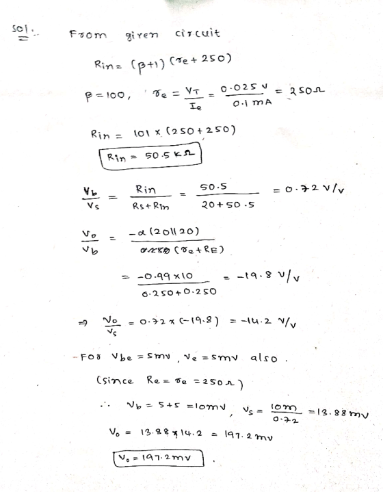
it of Fig. P6.120, the BJT is biased with nt source, and vsig is a small...
A CE amplifier utilizes a BJT with β = 100 biased at IC = 0.5 mA;...
A CE amplifier utilizes a BJT with β = 100 biased at IC = 0.5 mA; it has a collector resistance RC = 10 kΩ. Find Rin, Ro, and Avo. If the amplifier is fed with a signal source having a resistance of 10 kΩ, and a load resistance RL =10 kΩ is connected to the output terminal, find the resulting Av and Gv. If the peak voltage of the sine wave appearing between base and emitter is to be...
please answer this ASAP Answer the following questions for the below BJT amplifier circuit. Assume capacitors...
 please answer this ASAP
Answer the following questions for the below BJT amplifier circuit. Assume capacitors are short in the signal circuit. Use Vr 25 mV,B = 100, Vpo = 0.7 V, and Ignore the early effect in the bias and signal circuits Find the Bias parameters of the amplifier circuit a) b) Find the small signal parameters of the amplifier. c) Draw the small signal equivalent circuit. Find the open loop voltage gain (Ayo), voltage gain (A,), total circuit...
please answer this ASAP
Answer the following questions for the below BJT amplifier circuit. Assume capacitors are short in the signal circuit. Use Vr 25 mV,B = 100, Vpo = 0.7 V, and Ignore the early effect in the bias and signal circuits Find the Bias parameters of the amplifier circuit a) b) Find the small signal parameters of the amplifier. c) Draw the small signal equivalent circuit. Find the open loop voltage gain (Ayo), voltage gain (A,), total circuit...
7.53 For the circuit shown in Fig. P7.53, draw a complete small-signal equivalent circuit utilizing an...
 7.53 For the circuit shown in Fig. P7.53, draw a complete small-signal equivalent circuit utilizing an appropriate T model for the BJT (use a =0.99). Your circuit should show the values of all components, including the model parameters. What is the input resistance R ? Calculate the overall voltage gain (v,/v). (also find A, for this amp) sig +5 V RC 12 kΩ C2 RL 12 ΚΩ Rsig 75 N ) 0.33 mA Vsig Rin Figure P7.53
Design a BJT amplifier based on the specifications provided in the table below. Your design shoul...
 THE STEPS TO DO SO:
Design a BJT amplifier based on the specifications provided in the table below. Your design should be insensitive to β variations, and both the input and the output should be AC coupled as in Fig. 1. Supply Voltage, Vcc Load Resistance, RL Transistor's Current Gain, β Relative Variation of lc for VBE-0.7 ± 0.1 V 0-to-Peak Output Swing, Vo Voltage Gain, A Input Resistance, R THD for 5kHz IV (0-to-peak) Sine Wave Output Voltage, V。S5%...
THE STEPS TO DO SO:
Design a BJT amplifier based on the specifications provided in the table below. Your design should be insensitive to β variations, and both the input and the output should be AC coupled as in Fig. 1. Supply Voltage, Vcc Load Resistance, RL Transistor's Current Gain, β Relative Variation of lc for VBE-0.7 ± 0.1 V 0-to-Peak Output Swing, Vo Voltage Gain, A Input Resistance, R THD for 5kHz IV (0-to-peak) Sine Wave Output Voltage, V。S5%...
6.5 BI C2 Cl sig in 0 Design the bias circuit of the CE amplifier shown...
 6.5 BI C2 Cl sig in 0 Design the bias circuit of the CE amplifier shown to obtain IE= 0.5 mA and Vc= +6 V. Design for a dc voltage at the base of 5 V and a current through RB2 of 50 μΑ. Let Vcc-+15 V, β-100, and VBE 0.7 V. a) Specify the values of RBi, RB2, RE, and Rc b) Also give the values of the BJT small-signal parameters gm, rr , and ro at the bias...
please I need details l and....Debate Club | Offic A) Theoretical Design Design a common emitter BJT amplifier with the following requirements: -Rin-10 K2, and Ro-45 ㏀ (Neglect the Early voltage...
 please I need details
l and....Debate Club | Offic A) Theoretical Design Design a common emitter BJT amplifier with the following requirements: -Rin-10 K2, and Ro-45 ㏀ (Neglect the Early voltage Effect) Vo/Vsig- Gv-40 VIV or 32 dB " VCC-9 V V, IC-1mA, VCE-3.25V and β-100 RL-40 kQ, Rsige I ka, R 1-3R2, and C1-C2-1 μF Voc RC C2 R1 Rsig C1 RL R2 RE B) Verify your design using Orcad Capture Pspice by doing 1) AC sweep (frequency response):...
please I need details
l and....Debate Club | Offic A) Theoretical Design Design a common emitter BJT amplifier with the following requirements: -Rin-10 K2, and Ro-45 ㏀ (Neglect the Early voltage Effect) Vo/Vsig- Gv-40 VIV or 32 dB " VCC-9 V V, IC-1mA, VCE-3.25V and β-100 RL-40 kQ, Rsige I ka, R 1-3R2, and C1-C2-1 μF Voc RC C2 R1 Rsig C1 RL R2 RE B) Verify your design using Orcad Capture Pspice by doing 1) AC sweep (frequency response):...
6.108 (d) Section 6.5: Discrete-Circuit Amplifiers 6.107 Calculate overall voltage gain G, of a 3 mA/V, ro= = 1...
 6.108 (d)
Section 6.5: Discrete-Circuit Amplifiers 6.107 Calculate overall voltage gain G, of a 3 mA/V, ro= = 10 MS2. The amplifier is the common-source amplifier for which g 100 k2, RD 10 k2, and RG fed from a signal source with a Thevenin resistance of l M2, and the amplifier output is coupled of 20 k2 to a load resistance SIM 6.108 The NMOS transistor in the CS amplifier shown in Fig. P6.108 has V, = 0.7 V and...
6.108 (d)
Section 6.5: Discrete-Circuit Amplifiers 6.107 Calculate overall voltage gain G, of a 3 mA/V, ro= = 10 MS2. The amplifier is the common-source amplifier for which g 100 k2, RD 10 k2, and RG fed from a signal source with a Thevenin resistance of l M2, and the amplifier output is coupled of 20 k2 to a load resistance SIM 6.108 The NMOS transistor in the CS amplifier shown in Fig. P6.108 has V, = 0.7 V and...
can you do 4.83 Ar- Q Sea 100 V, what does the gain become? age at...
 can
you do 4.83
Ar- Q Sea 100 V, what does the gain become? age at the collector. (b) Replacing the transistor by its T model, da the small-signal equivalent circuit of the a plifier. Analyze the resulting circuit to dete mine the voltage gain t/ 04.81 Consider the CE amplifier circuit of Fig. 4.43(a). It is required to design the circuit (i.e., find values for I and Rc) to meet the following specifications: (a) R,5kn (b) the voltage gain...
can
you do 4.83
Ar- Q Sea 100 V, what does the gain become? age at the collector. (b) Replacing the transistor by its T model, da the small-signal equivalent circuit of the a plifier. Analyze the resulting circuit to dete mine the voltage gain t/ 04.81 Consider the CE amplifier circuit of Fig. 4.43(a). It is required to design the circuit (i.e., find values for I and Rc) to meet the following specifications: (a) R,5kn (b) the voltage gain...
(a) Determine R, R,, and R Assume gr1 (b) Determinei,,i,ふi4.is, is, and i,' alf in terms oft,. (Hini; Use the current-divider rule at the drain of Q,) (c) Determine v, t, and u, all in terms of...
 (a) Determine R, R,, and R Assume gr1 (b) Determinei,,i,ふi4.is, is, and i,' alf in terms oft,. (Hini; Use the current-divider rule at the drain of Q,) (c) Determine v, t, and u, all in terms of v, (d) If บุ is a 5-mV peak sine wave and RJ,-20, sketch and clearly label the waveforms of v, U, and t, D 7.68 Design the double-cascode current source shown in Fig. P7.68 to provide 0.2 mA and the largest possible sig-...
A common source amplifier circuit based on a single n-channel MOSFET is shown in Figure 4b. Assume that the transconductance gm-60 mS (equivalent to mA/ V) and drain source resistance, os,...
 A common source amplifier circuit based on a single n-channel MOSFET is shown in Figure 4b. Assume that the transconductance gm-60 mS (equivalent to mA/ V) and drain source resistance, os, is so large it may be neglected. 0) Calculate the open circuit voltage gain Av Yout/ Vis. i) The amplifier has a load of 10 k2. Determine the current gain Va. = 12 V 150k 4k3 Vout Vin 200k GND = 0 V Figure 4b a) State the name...
 please answer this ASAP
Answer the following questions for the below BJT amplifier circuit. Assume capacitors are short in the signal circuit. Use Vr 25 mV,B = 100, Vpo = 0.7 V, and Ignore the early effect in the bias and signal circuits Find the Bias parameters of the amplifier circuit a) b) Find the small signal parameters of the amplifier. c) Draw the small signal equivalent circuit. Find the open loop voltage gain (Ayo), voltage gain (A,), total circuit...
please answer this ASAP
Answer the following questions for the below BJT amplifier circuit. Assume capacitors are short in the signal circuit. Use Vr 25 mV,B = 100, Vpo = 0.7 V, and Ignore the early effect in the bias and signal circuits Find the Bias parameters of the amplifier circuit a) b) Find the small signal parameters of the amplifier. c) Draw the small signal equivalent circuit. Find the open loop voltage gain (Ayo), voltage gain (A,), total circuit...
 7.53 For the circuit shown in Fig. P7.53, draw a complete small-signal equivalent circuit utilizing an appropriate T model for the BJT (use a =0.99). Your circuit should show the values of all components, including the model parameters. What is the input resistance R ? Calculate the overall voltage gain (v,/v). (also find A, for this amp) sig +5 V RC 12 kΩ C2 RL 12 ΚΩ Rsig 75 N ) 0.33 mA Vsig Rin Figure P7.53
 THE STEPS TO DO SO:
Design a BJT amplifier based on the specifications provided in the table below. Your design should be insensitive to β variations, and both the input and the output should be AC coupled as in Fig. 1. Supply Voltage, Vcc Load Resistance, RL Transistor's Current Gain, β Relative Variation of lc for VBE-0.7 ± 0.1 V 0-to-Peak Output Swing, Vo Voltage Gain, A Input Resistance, R THD for 5kHz IV (0-to-peak) Sine Wave Output Voltage, V。S5%...
THE STEPS TO DO SO:
Design a BJT amplifier based on the specifications provided in the table below. Your design should be insensitive to β variations, and both the input and the output should be AC coupled as in Fig. 1. Supply Voltage, Vcc Load Resistance, RL Transistor's Current Gain, β Relative Variation of lc for VBE-0.7 ± 0.1 V 0-to-Peak Output Swing, Vo Voltage Gain, A Input Resistance, R THD for 5kHz IV (0-to-peak) Sine Wave Output Voltage, V。S5%...
 6.5 BI C2 Cl sig in 0 Design the bias circuit of the CE amplifier shown to obtain IE= 0.5 mA and Vc= +6 V. Design for a dc voltage at the base of 5 V and a current through RB2 of 50 μΑ. Let Vcc-+15 V, β-100, and VBE 0.7 V. a) Specify the values of RBi, RB2, RE, and Rc b) Also give the values of the BJT small-signal parameters gm, rr , and ro at the bias...
 please I need details
l and....Debate Club | Offic A) Theoretical Design Design a common emitter BJT amplifier with the following requirements: -Rin-10 K2, and Ro-45 ㏀ (Neglect the Early voltage Effect) Vo/Vsig- Gv-40 VIV or 32 dB " VCC-9 V V, IC-1mA, VCE-3.25V and β-100 RL-40 kQ, Rsige I ka, R 1-3R2, and C1-C2-1 μF Voc RC C2 R1 Rsig C1 RL R2 RE B) Verify your design using Orcad Capture Pspice by doing 1) AC sweep (frequency response):...
please I need details
l and....Debate Club | Offic A) Theoretical Design Design a common emitter BJT amplifier with the following requirements: -Rin-10 K2, and Ro-45 ㏀ (Neglect the Early voltage Effect) Vo/Vsig- Gv-40 VIV or 32 dB " VCC-9 V V, IC-1mA, VCE-3.25V and β-100 RL-40 kQ, Rsige I ka, R 1-3R2, and C1-C2-1 μF Voc RC C2 R1 Rsig C1 RL R2 RE B) Verify your design using Orcad Capture Pspice by doing 1) AC sweep (frequency response):...
 6.108 (d)
Section 6.5: Discrete-Circuit Amplifiers 6.107 Calculate overall voltage gain G, of a 3 mA/V, ro= = 10 MS2. The amplifier is the common-source amplifier for which g 100 k2, RD 10 k2, and RG fed from a signal source with a Thevenin resistance of l M2, and the amplifier output is coupled of 20 k2 to a load resistance SIM 6.108 The NMOS transistor in the CS amplifier shown in Fig. P6.108 has V, = 0.7 V and...
6.108 (d)
Section 6.5: Discrete-Circuit Amplifiers 6.107 Calculate overall voltage gain G, of a 3 mA/V, ro= = 10 MS2. The amplifier is the common-source amplifier for which g 100 k2, RD 10 k2, and RG fed from a signal source with a Thevenin resistance of l M2, and the amplifier output is coupled of 20 k2 to a load resistance SIM 6.108 The NMOS transistor in the CS amplifier shown in Fig. P6.108 has V, = 0.7 V and...
 can
you do 4.83
Ar- Q Sea 100 V, what does the gain become? age at the collector. (b) Replacing the transistor by its T model, da the small-signal equivalent circuit of the a plifier. Analyze the resulting circuit to dete mine the voltage gain t/ 04.81 Consider the CE amplifier circuit of Fig. 4.43(a). It is required to design the circuit (i.e., find values for I and Rc) to meet the following specifications: (a) R,5kn (b) the voltage gain...
can
you do 4.83
Ar- Q Sea 100 V, what does the gain become? age at the collector. (b) Replacing the transistor by its T model, da the small-signal equivalent circuit of the a plifier. Analyze the resulting circuit to dete mine the voltage gain t/ 04.81 Consider the CE amplifier circuit of Fig. 4.43(a). It is required to design the circuit (i.e., find values for I and Rc) to meet the following specifications: (a) R,5kn (b) the voltage gain...
 (a) Determine R, R,, and R Assume gr1 (b) Determinei,,i,ふi4.is, is, and i,' alf in terms oft,. (Hini; Use the current-divider rule at the drain of Q,) (c) Determine v, t, and u, all in terms of v, (d) If บุ is a 5-mV peak sine wave and RJ,-20, sketch and clearly label the waveforms of v, U, and t, D 7.68 Design the double-cascode current source shown in Fig. P7.68 to provide 0.2 mA and the largest possible sig-...
 A common source amplifier circuit based on a single n-channel MOSFET is shown in Figure 4b. Assume that the transconductance gm-60 mS (equivalent to mA/ V) and drain source resistance, os, is so large it may be neglected. 0) Calculate the open circuit voltage gain Av Yout/ Vis. i) The amplifier has a load of 10 k2. Determine the current gain Va. = 12 V 150k 4k3 Vout Vin 200k GND = 0 V Figure 4b a) State the name...
Most questions answered within 3 hours.
-
The blues made its way into many kinds of music. Eric Clapton,
The Beatles, and Elvis...
asked 1 hour ago -
8. A wave in a string has a wave function given by: y (x, t) =...
asked 22 minutes ago -
If you’re standing at the bottom of a hill and asked to evaluate
it while being...
asked 2 hours ago -
1. Which region has taken the lead in the world of
e-waste handling?
a) European Union...
asked 2 hours ago -
A 8.15- g bullet from a 9-mm pistol has a velocity of 366.0 m/s.
It strikes...
asked 3 hours ago -
The outstanding bonds of Alpha Extracts have a yield to maturity
of 7.4 percent and a...
asked 3 hours ago -
The Problem: The Case of the Harmonizing Vacations
Your CEO is exploring partnering with a European...
asked 5 hours ago -
A chemical equation is balanced by adding coefficients in front
of some formulas so that the...
asked 5 hours ago -
From the literature (reference your sources): What are the
lattice parameters of calcite and aragonite? Why...
asked 5 hours ago -
Your system is rejecting the question am asking which is
preceded by a case study. It...
asked 5 hours ago -
3. On January 2, 2000, Larry creates a trust with himself as
trustee. Larry as trustee...
asked 5 hours ago -
A member of the volleyball team spikes the ball. During this
process, she changes the velocity...
asked 5 hours ago