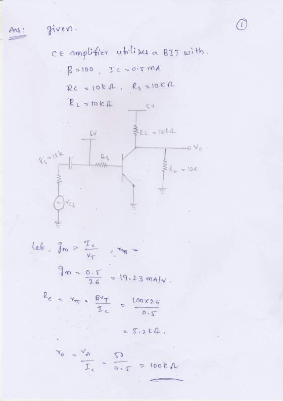
A CE amplifier utilizes a BJT with β = 100 biased at IC = 0.5 mA;...
A CE amplifier utilizes a BJT with β = 100 biased at IC = 0.5 mA; it has a collector resistance RC = 10 kΩ. Find Rin, Ro, and Avo. If the amplifier is fed with a signal source having a resistance of 10 kΩ, and a load resistance RL =10 kΩ is connected to the output terminal, find the resulting Av and Gv. If the peak voltage of the sine wave appearing between base and emitter is to be limited to 5 mV, what ?̂ sig is allowed, and what output voltage signal appears across the load? Hint: Avo = ?0 ?? (when load resistance is not included); Av = ?0 ?? (when load resistance is included) ; Gv = ?0 ???? (when load resistance is included)
Homework Answers
ANSWER
Given that
Bipolar junction transistor (BJT) : It is a type of semiconductor that uses both electron and hole charge carriers. They are used to amplify electric current. BJTs are available both alone or packaged into integrated circuits (ICs). BJTs are widely used in amplifiers for a large amount of everyday electronic equipment.A bipolar junction transistor is also known as a bipolar transistor.


Add Answer to:
A CE amplifier utilizes a BJT with β = 100 biased at IC = 0.5
mA;...
it of Fig. P6.120, the BJT is biased with nt source, and vsig is a small...
 it of Fig. P6.120, the BJT is biased with nt source, and vsig is a small sine-wave signal. Fi 6.120 In the circuit +3 V 20 kΩ 20 kΩ 20 kΩ 200 kΩ 0.1 mA Rin Figure P6.120 Find Rin and the gain terag. Assume β 100. If the amplitude of the signal Vbe is to be limited to 5 mV, what is the largest signal at the input? What is the corresponding signal at the output? sig
Problem 2: BJT Small-Signal Voltage Amplifiers in the lectures, we covered in detail the analysis of an npn BJT amplifier that utilizes a single-supply DC biasing. In this problem, you will meet...
 Problem 2: BJT Small-Signal Voltage Amplifiers in the lectures, we covered in detail the analysis of an npn BJT amplifier that utilizes a single-supply DC biasing. In this problem, you will meet two additional amplifier architectures- one that is based on dual DC supplies combined with a DC current source, and the other that utilizes a pnp BJT with single-supply biasing. In both problems (below) you need to manually find the amplifier's Q-point (that is, the DC values of Ic...
Problem 1.50 Design an amplifier that provides 0.5 W of signal power to a 100 Ω...
 Problem 1.50 Design an amplifier that provides 0.5 W of signal power to a 100 Ω load resistance. The signal source provides a 30 mV rms signal and has a resistance of 0.5 M2. There types of voltage- amplifier stages are available: A) A high-input-resistance type with Ri': 1 Mn, Avo-: 10, and Rout-: 10 kn B) A high-gain type with Rin 10 k2, Apo-100, and Rout 1 k2. C) A low-output-resistance type with Rin 10 kn, Avo 1, and...
Please show clear steps on how you got your answer. An NPN BJT with B =...
 Please show clear steps on how you got your answer.
An NPN BJT with B = 90 is used in a common-collector amplifier configuration and is biased such that IB = 90 uA with RL = 800 12. It is connected to an ac input signal with a signal resistance of 1 k 2. Assume that V1 = 25 mV and determine the overall voltage gain, Gv. OGV = 0.959 LOGv = 0.983 O Gv = 0.976 LOGY = 0.949
Please show clear steps on how you got your answer.
An NPN BJT with B = 90 is used in a common-collector amplifier configuration and is biased such that IB = 90 uA with RL = 800 12. It is connected to an ac input signal with a signal resistance of 1 k 2. Assume that V1 = 25 mV and determine the overall voltage gain, Gv. OGV = 0.959 LOGv = 0.983 O Gv = 0.976 LOGY = 0.949
2. CB amplifier is operating with RL Ic should the transistor be biased for the input resistance ...
 2. CB amplifier is operating with RL Ic should the transistor be biased for the input resistance Rin to equal that of the signal source? What is the resulting overall voltage gain? Assume α 1. 10 kQ, Rc 10 kQ, and Rs.,-50Ω. At what current
2. CB amplifier is operating with RL Ic should the transistor be biased for the input resistance Rin to equal that of the signal source? What is the resulting overall voltage gain? Assume α 1....
2. CB amplifier is operating with RL Ic should the transistor be biased for the input resistance Rin to equal that of the signal source? What is the resulting overall voltage gain? Assume α 1. 10 kQ, Rc 10 kQ, and Rs.,-50Ω. At what current
2. CB amplifier is operating with RL Ic should the transistor be biased for the input resistance Rin to equal that of the signal source? What is the resulting overall voltage gain? Assume α 1....
Design a BJT amplifier based on the specifications provided in the table below. Your design shoul...
 THE STEPS TO DO SO:
Design a BJT amplifier based on the specifications provided in the table below. Your design should be insensitive to β variations, and both the input and the output should be AC coupled as in Fig. 1. Supply Voltage, Vcc Load Resistance, RL Transistor's Current Gain, β Relative Variation of lc for VBE-0.7 ± 0.1 V 0-to-Peak Output Swing, Vo Voltage Gain, A Input Resistance, R THD for 5kHz IV (0-to-peak) Sine Wave Output Voltage, V。S5%...
THE STEPS TO DO SO:
Design a BJT amplifier based on the specifications provided in the table below. Your design should be insensitive to β variations, and both the input and the output should be AC coupled as in Fig. 1. Supply Voltage, Vcc Load Resistance, RL Transistor's Current Gain, β Relative Variation of lc for VBE-0.7 ± 0.1 V 0-to-Peak Output Swing, Vo Voltage Gain, A Input Resistance, R THD for 5kHz IV (0-to-peak) Sine Wave Output Voltage, V。S5%...
Problem 2: BJT Small-Signal Voltage Amplifiers In the lectures, we covered in detail the analysis...
 Problem 2: BJT Small-Signal Voltage Amplifiers In the lectures, we covered in detail the analysis of an npn BJT amplifier that utilizes a single-supply DC biasing. In this problem, you wi meet two additional amplifier architectures-one that is based on dual DC supplies combined with a DC current source, and the other that utilizes a pnp BJT with single-supply biasing In both problems (below) you need to manually find the amplifier's Q-point (that is, the DC values of Ic and...
The Final Project for the ELECTRONICS-1 course for, consists of designing a cascaded BJT Amplifier; using...
 The Final Project for the ELECTRONICS-1 course for, consists of
designing a cascaded BJT Amplifier; using 2 stages. The first stage
will be the Common Emitter (CE) Amplifier, the second stage is the
Common Collector (CC) Amplifier, as shown in the general diagram
below:
The overall amplification (voltage gain) Atotal =
98
The input source voltage Vsource is
an ideal source(Rs=0 Ohm) with peak voltage 10 mV,
and the source frequency
fsource =2K Hz
The load resistance RL = 47...
The Final Project for the ELECTRONICS-1 course for, consists of
designing a cascaded BJT Amplifier; using 2 stages. The first stage
will be the Common Emitter (CE) Amplifier, the second stage is the
Common Collector (CC) Amplifier, as shown in the general diagram
below:
The overall amplification (voltage gain) Atotal =
98
The input source voltage Vsource is
an ideal source(Rs=0 Ohm) with peak voltage 10 mV,
and the source frequency
fsource =2K Hz
The load resistance RL = 47...
FIND THE VALUES OF Rb1, Rb2, Re,Rc, rin , rout, overall gain and open circuit gain First, design a common emitter BJT a...
 FIND THE VALUES OF Rb1, Rb2, Re,Rc, rin , rout, overall gain and
open circuit gain
First, design a common emitter BJT amplifier Second, analyze the amplifier.( Avo, Gv, Rin, Rout) Third, compare your calculation with Multisim. Report must include comparison between your calculation & simulation results overall voltage gain, open circuit voltage gain, input resistance, and output resistance. This design project is not group work, must be done individually. Type your report. Design a discrete common emitter BJT amplifier.(Determine...
FIND THE VALUES OF Rb1, Rb2, Re,Rc, rin , rout, overall gain and
open circuit gain
First, design a common emitter BJT amplifier Second, analyze the amplifier.( Avo, Gv, Rin, Rout) Third, compare your calculation with Multisim. Report must include comparison between your calculation & simulation results overall voltage gain, open circuit voltage gain, input resistance, and output resistance. This design project is not group work, must be done individually. Type your report. Design a discrete common emitter BJT amplifier.(Determine...
6.5 BI C2 Cl sig in 0 Design the bias circuit of the CE amplifier shown...
 6.5 BI C2 Cl sig in 0 Design the bias circuit of the CE amplifier shown to obtain IE= 0.5 mA and Vc= +6 V. Design for a dc voltage at the base of 5 V and a current through RB2 of 50 μΑ. Let Vcc-+15 V, β-100, and VBE 0.7 V. a) Specify the values of RBi, RB2, RE, and Rc b) Also give the values of the BJT small-signal parameters gm, rr , and ro at the bias...
 it of Fig. P6.120, the BJT is biased with nt source, and vsig is a small sine-wave signal. Fi 6.120 In the circuit +3 V 20 kΩ 20 kΩ 20 kΩ 200 kΩ 0.1 mA Rin Figure P6.120 Find Rin and the gain terag. Assume β 100. If the amplitude of the signal Vbe is to be limited to 5 mV, what is the largest signal at the input? What is the corresponding signal at the output? sig
 Problem 2: BJT Small-Signal Voltage Amplifiers in the lectures, we covered in detail the analysis of an npn BJT amplifier that utilizes a single-supply DC biasing. In this problem, you will meet two additional amplifier architectures- one that is based on dual DC supplies combined with a DC current source, and the other that utilizes a pnp BJT with single-supply biasing. In both problems (below) you need to manually find the amplifier's Q-point (that is, the DC values of Ic...
 Problem 1.50 Design an amplifier that provides 0.5 W of signal power to a 100 Ω load resistance. The signal source provides a 30 mV rms signal and has a resistance of 0.5 M2. There types of voltage- amplifier stages are available: A) A high-input-resistance type with Ri': 1 Mn, Avo-: 10, and Rout-: 10 kn B) A high-gain type with Rin 10 k2, Apo-100, and Rout 1 k2. C) A low-output-resistance type with Rin 10 kn, Avo 1, and...
 Please show clear steps on how you got your answer.
An NPN BJT with B = 90 is used in a common-collector amplifier configuration and is biased such that IB = 90 uA with RL = 800 12. It is connected to an ac input signal with a signal resistance of 1 k 2. Assume that V1 = 25 mV and determine the overall voltage gain, Gv. OGV = 0.959 LOGv = 0.983 O Gv = 0.976 LOGY = 0.949
Please show clear steps on how you got your answer.
An NPN BJT with B = 90 is used in a common-collector amplifier configuration and is biased such that IB = 90 uA with RL = 800 12. It is connected to an ac input signal with a signal resistance of 1 k 2. Assume that V1 = 25 mV and determine the overall voltage gain, Gv. OGV = 0.959 LOGv = 0.983 O Gv = 0.976 LOGY = 0.949
 2. CB amplifier is operating with RL Ic should the transistor be biased for the input resistance Rin to equal that of the signal source? What is the resulting overall voltage gain? Assume α 1. 10 kQ, Rc 10 kQ, and Rs.,-50Ω. At what current
2. CB amplifier is operating with RL Ic should the transistor be biased for the input resistance Rin to equal that of the signal source? What is the resulting overall voltage gain? Assume α 1....
2. CB amplifier is operating with RL Ic should the transistor be biased for the input resistance Rin to equal that of the signal source? What is the resulting overall voltage gain? Assume α 1. 10 kQ, Rc 10 kQ, and Rs.,-50Ω. At what current
2. CB amplifier is operating with RL Ic should the transistor be biased for the input resistance Rin to equal that of the signal source? What is the resulting overall voltage gain? Assume α 1....
 THE STEPS TO DO SO:
Design a BJT amplifier based on the specifications provided in the table below. Your design should be insensitive to β variations, and both the input and the output should be AC coupled as in Fig. 1. Supply Voltage, Vcc Load Resistance, RL Transistor's Current Gain, β Relative Variation of lc for VBE-0.7 ± 0.1 V 0-to-Peak Output Swing, Vo Voltage Gain, A Input Resistance, R THD for 5kHz IV (0-to-peak) Sine Wave Output Voltage, V。S5%...
THE STEPS TO DO SO:
Design a BJT amplifier based on the specifications provided in the table below. Your design should be insensitive to β variations, and both the input and the output should be AC coupled as in Fig. 1. Supply Voltage, Vcc Load Resistance, RL Transistor's Current Gain, β Relative Variation of lc for VBE-0.7 ± 0.1 V 0-to-Peak Output Swing, Vo Voltage Gain, A Input Resistance, R THD for 5kHz IV (0-to-peak) Sine Wave Output Voltage, V。S5%...
 Problem 2: BJT Small-Signal Voltage Amplifiers In the lectures, we covered in detail the analysis of an npn BJT amplifier that utilizes a single-supply DC biasing. In this problem, you wi meet two additional amplifier architectures-one that is based on dual DC supplies combined with a DC current source, and the other that utilizes a pnp BJT with single-supply biasing In both problems (below) you need to manually find the amplifier's Q-point (that is, the DC values of Ic and...
 The Final Project for the ELECTRONICS-1 course for, consists of
designing a cascaded BJT Amplifier; using 2 stages. The first stage
will be the Common Emitter (CE) Amplifier, the second stage is the
Common Collector (CC) Amplifier, as shown in the general diagram
below:
The overall amplification (voltage gain) Atotal =
98
The input source voltage Vsource is
an ideal source(Rs=0 Ohm) with peak voltage 10 mV,
and the source frequency
fsource =2K Hz
The load resistance RL = 47...
The Final Project for the ELECTRONICS-1 course for, consists of
designing a cascaded BJT Amplifier; using 2 stages. The first stage
will be the Common Emitter (CE) Amplifier, the second stage is the
Common Collector (CC) Amplifier, as shown in the general diagram
below:
The overall amplification (voltage gain) Atotal =
98
The input source voltage Vsource is
an ideal source(Rs=0 Ohm) with peak voltage 10 mV,
and the source frequency
fsource =2K Hz
The load resistance RL = 47...
 FIND THE VALUES OF Rb1, Rb2, Re,Rc, rin , rout, overall gain and
open circuit gain
First, design a common emitter BJT amplifier Second, analyze the amplifier.( Avo, Gv, Rin, Rout) Third, compare your calculation with Multisim. Report must include comparison between your calculation & simulation results overall voltage gain, open circuit voltage gain, input resistance, and output resistance. This design project is not group work, must be done individually. Type your report. Design a discrete common emitter BJT amplifier.(Determine...
FIND THE VALUES OF Rb1, Rb2, Re,Rc, rin , rout, overall gain and
open circuit gain
First, design a common emitter BJT amplifier Second, analyze the amplifier.( Avo, Gv, Rin, Rout) Third, compare your calculation with Multisim. Report must include comparison between your calculation & simulation results overall voltage gain, open circuit voltage gain, input resistance, and output resistance. This design project is not group work, must be done individually. Type your report. Design a discrete common emitter BJT amplifier.(Determine...
 6.5 BI C2 Cl sig in 0 Design the bias circuit of the CE amplifier shown to obtain IE= 0.5 mA and Vc= +6 V. Design for a dc voltage at the base of 5 V and a current through RB2 of 50 μΑ. Let Vcc-+15 V, β-100, and VBE 0.7 V. a) Specify the values of RBi, RB2, RE, and Rc b) Also give the values of the BJT small-signal parameters gm, rr , and ro at the bias...
Most questions answered within 3 hours.
-
Let M = 8.00kg, m = 6.00kg, θ = 40.00, and the coefficient of
kinetic friction...
asked 3 seconds from now -
Java. For C through H True or false?
c. Primitive variables must be objects.
d. Integer...
asked 4 minutes ago -
Write a program that turns a 32-bit numeric value (e.g.,
0xFFFFh) and converts it to a...
asked 6 minutes ago -
A motor produces a torque of 0.25 N m at an angular velocity of
7200 revolutions...
asked 20 minutes ago -
***Please answer the below java question***
Are static methods inheritable? Can they be overridden?
asked 22 minutes ago -
In reaching her destination, a backpacker walks with an average
velocity of 1.13 m/s, due west....
asked 22 minutes ago -
Write two C programs that run a
server program and a client program concurrently.
Server program:...
asked 21 minutes ago -
Executive Program Practical Connection Assignment
Subject : Operations Security.
Assignment:
Provide a reflection of at least...
asked 31 minutes ago -
Every time Casey is at bat he has a 0.4 probability of
getting on base (assume...
asked 40 minutes ago -
The Walston Company is to be liquidated and has the following
liabilities:
Income taxes
$
9,400...
asked 46 minutes ago -
If
the more comprehensive data is available in MEPS, why does the NHIS
still exist? How...
asked 1 hour ago -
Koo argues that the Japanese economy in the 1990s suffered from
a balance sheet recession. What...
asked 1 hour ago