
Homework Answers


Add Answer to:
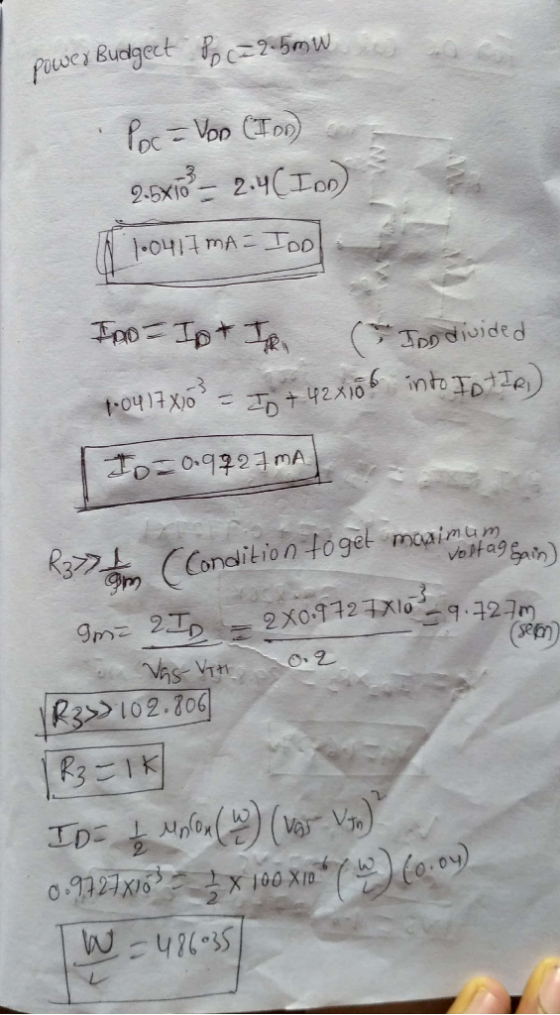
Design an amplifier that meets the following conditions. Determine the R3 value to get the maximum...
Please answer clearly Question 2 The amplifier shown in Figure 2 has the following parameters: Kn(W/L)-1 mA/V2, V-1 V Determine a) Voltage gain (Vo/vi) b) Input resistance (R) c) Output resistance (R...
 Please answer clearly
Question 2 The amplifier shown in Figure 2 has the following parameters: Kn(W/L)-1 mA/V2, V-1 V Determine a) Voltage gain (Vo/vi) b) Input resistance (R) c) Output resistance (Ro) d) Maximum output voltage swing so as the amplifier stays in saturation mode. Assume VDD-20 V, R1-2.5 ΚΩ, R2-1KQ, R3-0.5 ΚΩ, R4-5 MQ, R5_1ΜΩ. R4 R1 R5 R2 Ro R3
Question 2 The amplifier shown in Figure 2 has the following parameters: Kn(W/L)-1 mA/V2, V-1 V Determine a)...
Please answer clearly
Question 2 The amplifier shown in Figure 2 has the following parameters: Kn(W/L)-1 mA/V2, V-1 V Determine a) Voltage gain (Vo/vi) b) Input resistance (R) c) Output resistance (Ro) d) Maximum output voltage swing so as the amplifier stays in saturation mode. Assume VDD-20 V, R1-2.5 ΚΩ, R2-1KQ, R3-0.5 ΚΩ, R4-5 MQ, R5_1ΜΩ. R4 R1 R5 R2 Ro R3
Question 2 The amplifier shown in Figure 2 has the following parameters: Kn(W/L)-1 mA/V2, V-1 V Determine a)...
5. (20 points) For the amplifier in the following figure: +Vcc Rout Rc C3 R2 Rin Ri 1 k R3 Vo Vi R1 RE -VEE a) Draw the de equivalent circuit and find the Q-point. Assume B -75 b) Draw the equiv...
 5. (20 points) For the amplifier in the following figure: +Vcc Rout Rc C3 R2 Rin Ri 1 k R3 Vo Vi R1 RE -VEE a) Draw the de equivalent circuit and find the Q-point. Assume B -75 b) Draw the equivalent circuit used for ac analysis. Find the values in Thevenin equivalent representation for the amplifiers between C, and C as shown below. What is the maximum value of v, that satisfies the small- signal assumption? Rout Ri vi...
1. Design the common source amplifier shown in Figure 1 with Ip- 1 mA and Vo 5 V Determine V2 and Ri. The MOSFET characteristics are V-50 V, k-0.093 A/V, gate-to- drain capacitance, Cd 40 pF,...
 1. Design the common source amplifier shown in Figure 1 with Ip- 1 mA and Vo 5 V Determine V2 and Ri. The MOSFET characteristics are V-50 V, k-0.093 A/V, gate-to- drain capacitance, Cd 40 pF, and Vi 1.1 V. (For PSpice simulations, use parameters: VTO. 1.1 LAMBDA-002 KP-0.093 CGDO-4E-7 w=100u L-I00u for the 2N7000 MOSFET.) a. Determine the gain and gm of the circuit b. Determine the low-frequency (high-pass response) poles of the common-source amplifier due to the coupling...
Problem 3: Design Problem On Figure P3a, you have a Common Source (CS) n-channel MOSFET amplifier....
 Problem 3: Design Problem On Figure P3a, you have a Common Source (CS) n-channel MOSFET amplifier. Notice the absence of a source resistor Rsig and load resistor R. If we know how the present amplifier (the one on Figure P3a) behaves without Rsig and RL, we can infer its behaviors if Rsig and R were to be added. design the amplifier circuit on Figure P3a, i.e., you have to find appropriate values for RGj You are to RG,, RD, and...
7. (2 pts) For the following write the equation for the voltage SKO 10 O C...
 7. (2 pts) For the following write the equation for the voltage SKO 10 O C 20 uF across the capacitor 8. (2 pts) The source voltage vs in the circuit below is -640 mV. What range of Rx allows the inverting amplifier to operate in its linear region? 16k NOV 9. (2 pts) Suppose we wish to amplify a voltage vg, such that - 1.5V sv, 1.5V. What are the smallest power supply voltages that could be used and...
A common source amplifier circuit based on a single n-channel MOSFET is shown in Figure 4b. Assume that the transconductance gm-60 mS (equivalent to mA/ V) and drain source resistance, os,...
 A common source amplifier circuit based on a single n-channel MOSFET is shown in Figure 4b. Assume that the transconductance gm-60 mS (equivalent to mA/ V) and drain source resistance, os, is so large it may be neglected. 0) Calculate the open circuit voltage gain Av Yout/ Vis. i) The amplifier has a load of 10 k2. Determine the current gain Va. = 12 V 150k 4k3 Vout Vin 200k GND = 0 V Figure 4b a) State the name...
I need a help with my lab, I write all data that get. 355 SERIES SINUSOIDAL...
 I need a help with my lab, I write all data that get.
355 SERIES SINUSOIDAL CIRCU CUITS neeseed 000 10 mH 10 kHz + R E-8V(Pp) V 1 kn Channel 2 Vert: 1 Vidiv Hor: 20 us/div. Channel 1 Vert: 1 Vidiv Hor: 20 us/div. FIG. 9.1 (b) After setting E to 8 V (p-p), determine the peak-to-peak voltage for Ve from chan- nel 2 and record in the top row of Table 9.1 Determine the phase angle 8,...
I need a help with my lab, I write all data that get.
355 SERIES SINUSOIDAL CIRCU CUITS neeseed 000 10 mH 10 kHz + R E-8V(Pp) V 1 kn Channel 2 Vert: 1 Vidiv Hor: 20 us/div. Channel 1 Vert: 1 Vidiv Hor: 20 us/div. FIG. 9.1 (b) After setting E to 8 V (p-p), determine the peak-to-peak voltage for Ve from chan- nel 2 and record in the top row of Table 9.1 Determine the phase angle 8,...
 Please answer clearly
Question 2 The amplifier shown in Figure 2 has the following parameters: Kn(W/L)-1 mA/V2, V-1 V Determine a) Voltage gain (Vo/vi) b) Input resistance (R) c) Output resistance (Ro) d) Maximum output voltage swing so as the amplifier stays in saturation mode. Assume VDD-20 V, R1-2.5 ΚΩ, R2-1KQ, R3-0.5 ΚΩ, R4-5 MQ, R5_1ΜΩ. R4 R1 R5 R2 Ro R3
Question 2 The amplifier shown in Figure 2 has the following parameters: Kn(W/L)-1 mA/V2, V-1 V Determine a)...
Please answer clearly
Question 2 The amplifier shown in Figure 2 has the following parameters: Kn(W/L)-1 mA/V2, V-1 V Determine a) Voltage gain (Vo/vi) b) Input resistance (R) c) Output resistance (Ro) d) Maximum output voltage swing so as the amplifier stays in saturation mode. Assume VDD-20 V, R1-2.5 ΚΩ, R2-1KQ, R3-0.5 ΚΩ, R4-5 MQ, R5_1ΜΩ. R4 R1 R5 R2 Ro R3
Question 2 The amplifier shown in Figure 2 has the following parameters: Kn(W/L)-1 mA/V2, V-1 V Determine a)...
 5. (20 points) For the amplifier in the following figure: +Vcc Rout Rc C3 R2 Rin Ri 1 k R3 Vo Vi R1 RE -VEE a) Draw the de equivalent circuit and find the Q-point. Assume B -75 b) Draw the equivalent circuit used for ac analysis. Find the values in Thevenin equivalent representation for the amplifiers between C, and C as shown below. What is the maximum value of v, that satisfies the small- signal assumption? Rout Ri vi...
 1. Design the common source amplifier shown in Figure 1 with Ip- 1 mA and Vo 5 V Determine V2 and Ri. The MOSFET characteristics are V-50 V, k-0.093 A/V, gate-to- drain capacitance, Cd 40 pF, and Vi 1.1 V. (For PSpice simulations, use parameters: VTO. 1.1 LAMBDA-002 KP-0.093 CGDO-4E-7 w=100u L-I00u for the 2N7000 MOSFET.) a. Determine the gain and gm of the circuit b. Determine the low-frequency (high-pass response) poles of the common-source amplifier due to the coupling...
 Problem 3: Design Problem On Figure P3a, you have a Common Source (CS) n-channel MOSFET amplifier. Notice the absence of a source resistor Rsig and load resistor R. If we know how the present amplifier (the one on Figure P3a) behaves without Rsig and RL, we can infer its behaviors if Rsig and R were to be added. design the amplifier circuit on Figure P3a, i.e., you have to find appropriate values for RGj You are to RG,, RD, and...
 7. (2 pts) For the following write the equation for the voltage SKO 10 O C 20 uF across the capacitor 8. (2 pts) The source voltage vs in the circuit below is -640 mV. What range of Rx allows the inverting amplifier to operate in its linear region? 16k NOV 9. (2 pts) Suppose we wish to amplify a voltage vg, such that - 1.5V sv, 1.5V. What are the smallest power supply voltages that could be used and...
 A common source amplifier circuit based on a single n-channel MOSFET is shown in Figure 4b. Assume that the transconductance gm-60 mS (equivalent to mA/ V) and drain source resistance, os, is so large it may be neglected. 0) Calculate the open circuit voltage gain Av Yout/ Vis. i) The amplifier has a load of 10 k2. Determine the current gain Va. = 12 V 150k 4k3 Vout Vin 200k GND = 0 V Figure 4b a) State the name...
 I need a help with my lab, I write all data that get.
355 SERIES SINUSOIDAL CIRCU CUITS neeseed 000 10 mH 10 kHz + R E-8V(Pp) V 1 kn Channel 2 Vert: 1 Vidiv Hor: 20 us/div. Channel 1 Vert: 1 Vidiv Hor: 20 us/div. FIG. 9.1 (b) After setting E to 8 V (p-p), determine the peak-to-peak voltage for Ve from chan- nel 2 and record in the top row of Table 9.1 Determine the phase angle 8,...
I need a help with my lab, I write all data that get.
355 SERIES SINUSOIDAL CIRCU CUITS neeseed 000 10 mH 10 kHz + R E-8V(Pp) V 1 kn Channel 2 Vert: 1 Vidiv Hor: 20 us/div. Channel 1 Vert: 1 Vidiv Hor: 20 us/div. FIG. 9.1 (b) After setting E to 8 V (p-p), determine the peak-to-peak voltage for Ve from chan- nel 2 and record in the top row of Table 9.1 Determine the phase angle 8,...
Most questions answered within 3 hours.
-
Which types of mutations in DNA can lead to the translation of a
non-functional protein product?...
asked 1 minute from now -
Many structures are composed of individual elements that react
in unison when forces are applied. the...
asked 1 second from now -
Work of 1950 J is done by stirring a perfectly insulated beaker
containing 75 g of...
asked 29 minutes ago -
The neighborhood kids set up an outdoor lemonade stand in
Maryland in June. They find that...
asked 31 minutes ago -
9. A company has a beginning inventory of 4,000 units. The
company estimates it will sell...
asked 44 minutes ago -
A patient goes to the doctor's office with symptoms of a urinary
tract infection and provides...
asked 46 minutes ago -
When responding to the essay questions, be sure to cite any
material you obtained from a...
asked 46 minutes ago -
The energy of an electron in a 2.25-eV-deep potential well is
1.50 eV.At what distance into...
asked 48 minutes ago -
Q1:Which three evolutionary innovations are present in land
plants (but not all land plants) that allowed...
asked 51 minutes ago -
Lymphosarcoma is
extremely rare. Risk factors for the disease are largely unknown.
What kind of study...
asked 53 minutes ago -
The solubility of benzoic acid in water is:
0.29g/100mL at 20°C
6.8g/100mL at 100°C
a) What...
asked 55 minutes ago -
Which food law was passed in 1996 and changed how pesticide
residues on food were regulated...
asked 1 hour ago