
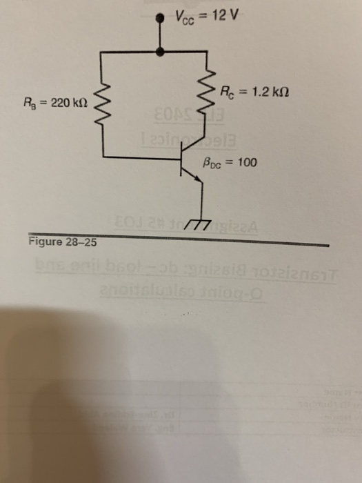
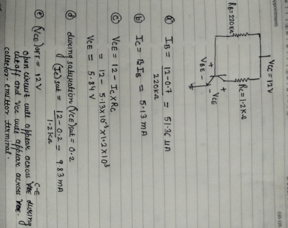
Vcc = 12 V R 1.2 kn Rg=220 k Boc 100 EOJ 2 77pieaA Figure 28-25 ba eall bsol-ot enotsloalso anioc-o daiansi
Homework Answers
Add Answer to:
28-29 In Fig. 28-25, solve for the following: a. I8 b.Ic c. VCE OS d. Icisaty...
28-28 What form of bias is shown in Fig. 28-25? VcC= 12 V Rc 1.2 kn...
 28-28 What form of bias is shown in Fig. 28-25? VcC= 12 V Rc 1.2 kn Rg=220 k EOASH Boc = 100 EOO T77siea A Figure 28-25 bs enil bsotob nlesia otalans anoitslualso aniog-O
28-28 What form of bias is shown in Fig. 28-25? VcC= 12 V Rc 1.2 kn Rg=220 k EOASH Boc = 100 EOO T77siea A Figure 28-25 bs enil bsotob nlesia otalans anoitslualso aniog-O
28-28 What form of bias is shown in Fig. 28-25? VcC= 12 V Rc 1.2 kn Rg=220 k EOASH Boc = 100 EOO T77siea A Figure 28-25 bs enil bsotob nlesia otalans anoitslualso aniog-O
What type of transistor amplifier is shown in Fig. 29-19a? 29-3 +Vcc 15 V = 7.5...
 What type of transistor amplifier is shown in Fig. 29-19a? 29-3 +Vcc 15 V = 7.5 k R= 1.2 k R, C B= 100 2 = 1.5 k° in 10 mV RE = 360 CE (a) Calculate the following DC quantities in Fig. 29-19a: 29-4 Ves a. b. VE C. d. Vc e. VCE W
What type of transistor amplifier is shown in Fig. 29-19a? 29-3 +Vcc 15 V = 7.5 k R= 1.2 k R, C B= 100 2...
What type of transistor amplifier is shown in Fig. 29-19a? 29-3 +Vcc 15 V = 7.5 k R= 1.2 k R, C B= 100 2 = 1.5 k° in 10 mV RE = 360 CE (a) Calculate the following DC quantities in Fig. 29-19a: 29-4 Ves a. b. VE C. d. Vc e. VCE W
What type of transistor amplifier is shown in Fig. 29-19a? 29-3 +Vcc 15 V = 7.5 k R= 1.2 k R, C B= 100 2...
for the collector feedback configuration of fig 5.167 Collector Feedback Configuration 5.10 29. For the collector...
 for the collector feedback configuration of fig 5.167
Collector Feedback Configuration 5.10 29. For the collector feedback configuration of Fig. 5.167: a. Determine r b. Find Z, and Z c. Calculate Ay 19 for the network of Fig. 5.168, deter- 30. Given r,10 , B 200, A, =-160, and A mine Rc, RF, and Vcc *31. For the network of Fig. 5.49 a. Derive the approximate equation for A b. Derive the approximate equations for Z, and Zp c. Given...
for the collector feedback configuration of fig 5.167
Collector Feedback Configuration 5.10 29. For the collector feedback configuration of Fig. 5.167: a. Determine r b. Find Z, and Z c. Calculate Ay 19 for the network of Fig. 5.168, deter- 30. Given r,10 , B 200, A, =-160, and A mine Rc, RF, and Vcc *31. For the network of Fig. 5.49 a. Derive the approximate equation for A b. Derive the approximate equations for Z, and Zp c. Given...
1.(TCO 2) For the circuit in the following figure (Chapter 3, Figure 3-29, on page 135),...
 1.(TCO 2) For the circuit in the following figure (Chapter 3,
Figure 3-29, on page 135), VCC=18
V, R1=10 K?, R2=2.2
K?, RC=1
k?, RE1=220
?,RE2=220 ?, RL=10
K?, Rs=1 K?VCC=18 V,
R1=10 K?, R2=2.2 K?, RC=1 k?, RE1=220
?,RE2=220 ?, RL=10 K?, Rs=1 K? . Determine
the AC voltage gain.
2.(TCO 2) For the circuit in the following figure (Chapter 3,
Figure 3-29, on page 135), VCC=18
V, R1=10 K?, R2=2.2
K?, RC=3
k?, RE1=220
?,RE2=220 ?, RL=5
K?, Rs=1 K?VCC=18 V,
R1=10 K?, R2=2.2 K?, RC=3 k?, RE1=220
?,RE2=220 ?, RL=5 K?, Rs=1 K?...
1.(TCO 2) For the circuit in the following figure (Chapter 3,
Figure 3-29, on page 135), VCC=18
V, R1=10 K?, R2=2.2
K?, RC=1
k?, RE1=220
?,RE2=220 ?, RL=10
K?, Rs=1 K?VCC=18 V,
R1=10 K?, R2=2.2 K?, RC=1 k?, RE1=220
?,RE2=220 ?, RL=10 K?, Rs=1 K? . Determine
the AC voltage gain.
2.(TCO 2) For the circuit in the following figure (Chapter 3,
Figure 3-29, on page 135), VCC=18
V, R1=10 K?, R2=2.2
K?, RC=3
k?, RE1=220
?,RE2=220 ?, RL=5
K?, Rs=1 K?VCC=18 V,
R1=10 K?, R2=2.2 K?, RC=3 k?, RE1=220
?,RE2=220 ?, RL=5 K?, Rs=1 K?...
Determine Av for the following circuit. +15 V Rc C 2.2 k 22 kΩ Ci Boc 90 β-100 R2 4.7 kΩ 1.0 k12 ...
 Determine Av for the following circuit. +15 V Rc C 2.2 k 22 kΩ Ci Boc 90 β-100 R2 4.7 kΩ 1.0 k12 AS Determine Ap of the emitter-follower in the figure below. Assume (beta 175) Vce +10 V 18 kn Ci 2N3904 I V rms C2 10 pF 1.0kΩ 10kn Fint eo r gure below (beta 250) Cc +10 V Rc 2.2kD Ri 2N3904 okn 100 pF R 2k010kn
Determine Av for the following circuit. +15 V Rc C...
Determine Av for the following circuit. +15 V Rc C 2.2 k 22 kΩ Ci Boc 90 β-100 R2 4.7 kΩ 1.0 k12 AS Determine Ap of the emitter-follower in the figure below. Assume (beta 175) Vce +10 V 18 kn Ci 2N3904 I V rms C2 10 pF 1.0kΩ 10kn Fint eo r gure below (beta 250) Cc +10 V Rc 2.2kD Ri 2N3904 okn 100 pF R 2k010kn
Determine Av for the following circuit. +15 V Rc C...
1. Design the common-emitter amplifier in Fig. 4(a) with the following specifications: Supply Vol...
 Figure 4. (a)
1. Design the common-emitter amplifier in Fig. 4(a) with the following specifications: Supply Voltage, Vcc 0-to-Peak Output Swing, V Voltage Gain, A. Input Resistance, R Output Resistance, Ro THD for 5kHz 1 V (0-to-peak) Sine Wave Output Voltage, V Relative Variation of Ic for VBE 0.7t 0.1V Transistor's Current Gain, β 5V 25 1.8kS2 4% 10% 100 Show your design procedure and all your calculations. Your design should be insensitive to B variations. Vcc RB1 Rc 0...
Figure 4. (a)
1. Design the common-emitter amplifier in Fig. 4(a) with the following specifications: Supply Voltage, Vcc 0-to-Peak Output Swing, V Voltage Gain, A. Input Resistance, R Output Resistance, Ro THD for 5kHz 1 V (0-to-peak) Sine Wave Output Voltage, V Relative Variation of Ic for VBE 0.7t 0.1V Transistor's Current Gain, β 5V 25 1.8kS2 4% 10% 100 Show your design procedure and all your calculations. Your design should be insensitive to B variations. Vcc RB1 Rc 0...
Solve each practice problem. TYPE solutions in engineering notation TYPE solutions in engineering notation. Calcula...
 Solve each practice problem. TYPE solutions in
engineering notation
TYPE solutions in engineering
notation.
Calculate the component voltages and branch currents for the circuit shown in Figure 6.40, along with the values of I, and Rr. 3. R3 2 kn R4 4.7 k R1 10 k Vs 26 V R5 3.3 k R2 3 kn FIGURE 6.40 Calculate the component currents and loop voltages for the circuit shown in Figure 6.42, along with the values of I and Rr 5....
Solve each practice problem. TYPE solutions in
engineering notation
TYPE solutions in engineering
notation.
Calculate the component voltages and branch currents for the circuit shown in Figure 6.40, along with the values of I, and Rr. 3. R3 2 kn R4 4.7 k R1 10 k Vs 26 V R5 3.3 k R2 3 kn FIGURE 6.40 Calculate the component currents and loop voltages for the circuit shown in Figure 6.42, along with the values of I and Rr 5....
Please solve the following problem. 6-33 In Fig. 6-43, solve for , R R2, V2, V,...
 Please solve the following problem.
6-33 In Fig. 6-43, solve for , R R2, V2, V, V, , Vo, 2 /3 l 5 and l Figure 6-43 V,=5.4 V R1 = 180 Ω P/2 K. = 30 V 4 1.5 kΩ Re-100 Ω
Please solve the following problem.
6-33 In Fig. 6-43, solve for , R R2, V2, V, V, , Vo, 2 /3 l 5 and l Figure 6-43 V,=5.4 V R1 = 180 Ω P/2 K. = 30 V 4 1.5 kΩ Re-100 Ω
Please provide an example on how to solve this problem. 1. In the circuit of Fig.2,...
 Please provide an example on how to solve this problem.
1. In the circuit of Fig.2, load resistance R = 30 ? and line resistance r varies from o to 100 2.Draw the graph of absorbed power PR with respect to R. V- 12 Volt. Use the data Table below. In the plot, R will be in r axis and PR will be in y axis Fig. 2. A power supply with internal resistanc r is connected with load resistance...
Please provide an example on how to solve this problem.
1. In the circuit of Fig.2, load resistance R = 30 ? and line resistance r varies from o to 100 2.Draw the graph of absorbed power PR with respect to R. V- 12 Volt. Use the data Table below. In the plot, R will be in r axis and PR will be in y axis Fig. 2. A power supply with internal resistanc r is connected with load resistance...
23 24 25 26 27 28 29 30 - 31 32 33 34 In the Periodic...
 23 24 25 26 27 28 29 30 - 31 32 33 34 In the Periodic Table below, shade all the elements for which the neutral atom has a valence electron configuration of n s mp', where n stands for an integer. H Li Be Na Mg K Ca Sc Rb Sr Y Cs Ba La Fr Ra Ac He BC N O F Ne Al Si P S Clar TV Cr Mn Fe Co Ni Cu Zn Ga Ge...
 28-28 What form of bias is shown in Fig. 28-25? VcC= 12 V Rc 1.2 kn Rg=220 k EOASH Boc = 100 EOO T77siea A Figure 28-25 bs enil bsotob nlesia otalans anoitslualso aniog-O
28-28 What form of bias is shown in Fig. 28-25? VcC= 12 V Rc 1.2 kn Rg=220 k EOASH Boc = 100 EOO T77siea A Figure 28-25 bs enil bsotob nlesia otalans anoitslualso aniog-O
28-28 What form of bias is shown in Fig. 28-25? VcC= 12 V Rc 1.2 kn Rg=220 k EOASH Boc = 100 EOO T77siea A Figure 28-25 bs enil bsotob nlesia otalans anoitslualso aniog-O
 What type of transistor amplifier is shown in Fig. 29-19a? 29-3 +Vcc 15 V = 7.5 k R= 1.2 k R, C B= 100 2 = 1.5 k° in 10 mV RE = 360 CE (a) Calculate the following DC quantities in Fig. 29-19a: 29-4 Ves a. b. VE C. d. Vc e. VCE W
What type of transistor amplifier is shown in Fig. 29-19a? 29-3 +Vcc 15 V = 7.5 k R= 1.2 k R, C B= 100 2...
What type of transistor amplifier is shown in Fig. 29-19a? 29-3 +Vcc 15 V = 7.5 k R= 1.2 k R, C B= 100 2 = 1.5 k° in 10 mV RE = 360 CE (a) Calculate the following DC quantities in Fig. 29-19a: 29-4 Ves a. b. VE C. d. Vc e. VCE W
What type of transistor amplifier is shown in Fig. 29-19a? 29-3 +Vcc 15 V = 7.5 k R= 1.2 k R, C B= 100 2...
 for the collector feedback configuration of fig 5.167
Collector Feedback Configuration 5.10 29. For the collector feedback configuration of Fig. 5.167: a. Determine r b. Find Z, and Z c. Calculate Ay 19 for the network of Fig. 5.168, deter- 30. Given r,10 , B 200, A, =-160, and A mine Rc, RF, and Vcc *31. For the network of Fig. 5.49 a. Derive the approximate equation for A b. Derive the approximate equations for Z, and Zp c. Given...
for the collector feedback configuration of fig 5.167
Collector Feedback Configuration 5.10 29. For the collector feedback configuration of Fig. 5.167: a. Determine r b. Find Z, and Z c. Calculate Ay 19 for the network of Fig. 5.168, deter- 30. Given r,10 , B 200, A, =-160, and A mine Rc, RF, and Vcc *31. For the network of Fig. 5.49 a. Derive the approximate equation for A b. Derive the approximate equations for Z, and Zp c. Given...
 1.(TCO 2) For the circuit in the following figure (Chapter 3,
Figure 3-29, on page 135), VCC=18
V, R1=10 K?, R2=2.2
K?, RC=1
k?, RE1=220
?,RE2=220 ?, RL=10
K?, Rs=1 K?VCC=18 V,
R1=10 K?, R2=2.2 K?, RC=1 k?, RE1=220
?,RE2=220 ?, RL=10 K?, Rs=1 K? . Determine
the AC voltage gain.
2.(TCO 2) For the circuit in the following figure (Chapter 3,
Figure 3-29, on page 135), VCC=18
V, R1=10 K?, R2=2.2
K?, RC=3
k?, RE1=220
?,RE2=220 ?, RL=5
K?, Rs=1 K?VCC=18 V,
R1=10 K?, R2=2.2 K?, RC=3 k?, RE1=220
?,RE2=220 ?, RL=5 K?, Rs=1 K?...
1.(TCO 2) For the circuit in the following figure (Chapter 3,
Figure 3-29, on page 135), VCC=18
V, R1=10 K?, R2=2.2
K?, RC=1
k?, RE1=220
?,RE2=220 ?, RL=10
K?, Rs=1 K?VCC=18 V,
R1=10 K?, R2=2.2 K?, RC=1 k?, RE1=220
?,RE2=220 ?, RL=10 K?, Rs=1 K? . Determine
the AC voltage gain.
2.(TCO 2) For the circuit in the following figure (Chapter 3,
Figure 3-29, on page 135), VCC=18
V, R1=10 K?, R2=2.2
K?, RC=3
k?, RE1=220
?,RE2=220 ?, RL=5
K?, Rs=1 K?VCC=18 V,
R1=10 K?, R2=2.2 K?, RC=3 k?, RE1=220
?,RE2=220 ?, RL=5 K?, Rs=1 K?...
 Determine Av for the following circuit. +15 V Rc C 2.2 k 22 kΩ Ci Boc 90 β-100 R2 4.7 kΩ 1.0 k12 AS Determine Ap of the emitter-follower in the figure below. Assume (beta 175) Vce +10 V 18 kn Ci 2N3904 I V rms C2 10 pF 1.0kΩ 10kn Fint eo r gure below (beta 250) Cc +10 V Rc 2.2kD Ri 2N3904 okn 100 pF R 2k010kn
Determine Av for the following circuit. +15 V Rc C...
Determine Av for the following circuit. +15 V Rc C 2.2 k 22 kΩ Ci Boc 90 β-100 R2 4.7 kΩ 1.0 k12 AS Determine Ap of the emitter-follower in the figure below. Assume (beta 175) Vce +10 V 18 kn Ci 2N3904 I V rms C2 10 pF 1.0kΩ 10kn Fint eo r gure below (beta 250) Cc +10 V Rc 2.2kD Ri 2N3904 okn 100 pF R 2k010kn
Determine Av for the following circuit. +15 V Rc C...
 Figure 4. (a)
1. Design the common-emitter amplifier in Fig. 4(a) with the following specifications: Supply Voltage, Vcc 0-to-Peak Output Swing, V Voltage Gain, A. Input Resistance, R Output Resistance, Ro THD for 5kHz 1 V (0-to-peak) Sine Wave Output Voltage, V Relative Variation of Ic for VBE 0.7t 0.1V Transistor's Current Gain, β 5V 25 1.8kS2 4% 10% 100 Show your design procedure and all your calculations. Your design should be insensitive to B variations. Vcc RB1 Rc 0...
Figure 4. (a)
1. Design the common-emitter amplifier in Fig. 4(a) with the following specifications: Supply Voltage, Vcc 0-to-Peak Output Swing, V Voltage Gain, A. Input Resistance, R Output Resistance, Ro THD for 5kHz 1 V (0-to-peak) Sine Wave Output Voltage, V Relative Variation of Ic for VBE 0.7t 0.1V Transistor's Current Gain, β 5V 25 1.8kS2 4% 10% 100 Show your design procedure and all your calculations. Your design should be insensitive to B variations. Vcc RB1 Rc 0...
 Solve each practice problem. TYPE solutions in
engineering notation
TYPE solutions in engineering
notation.
Calculate the component voltages and branch currents for the circuit shown in Figure 6.40, along with the values of I, and Rr. 3. R3 2 kn R4 4.7 k R1 10 k Vs 26 V R5 3.3 k R2 3 kn FIGURE 6.40 Calculate the component currents and loop voltages for the circuit shown in Figure 6.42, along with the values of I and Rr 5....
Solve each practice problem. TYPE solutions in
engineering notation
TYPE solutions in engineering
notation.
Calculate the component voltages and branch currents for the circuit shown in Figure 6.40, along with the values of I, and Rr. 3. R3 2 kn R4 4.7 k R1 10 k Vs 26 V R5 3.3 k R2 3 kn FIGURE 6.40 Calculate the component currents and loop voltages for the circuit shown in Figure 6.42, along with the values of I and Rr 5....
 Please solve the following problem.
6-33 In Fig. 6-43, solve for , R R2, V2, V, V, , Vo, 2 /3 l 5 and l Figure 6-43 V,=5.4 V R1 = 180 Ω P/2 K. = 30 V 4 1.5 kΩ Re-100 Ω
Please solve the following problem.
6-33 In Fig. 6-43, solve for , R R2, V2, V, V, , Vo, 2 /3 l 5 and l Figure 6-43 V,=5.4 V R1 = 180 Ω P/2 K. = 30 V 4 1.5 kΩ Re-100 Ω
 Please provide an example on how to solve this problem.
1. In the circuit of Fig.2, load resistance R = 30 ? and line resistance r varies from o to 100 2.Draw the graph of absorbed power PR with respect to R. V- 12 Volt. Use the data Table below. In the plot, R will be in r axis and PR will be in y axis Fig. 2. A power supply with internal resistanc r is connected with load resistance...
Please provide an example on how to solve this problem.
1. In the circuit of Fig.2, load resistance R = 30 ? and line resistance r varies from o to 100 2.Draw the graph of absorbed power PR with respect to R. V- 12 Volt. Use the data Table below. In the plot, R will be in r axis and PR will be in y axis Fig. 2. A power supply with internal resistanc r is connected with load resistance...
 23 24 25 26 27 28 29 30 - 31 32 33 34 In the Periodic Table below, shade all the elements for which the neutral atom has a valence electron configuration of n s mp', where n stands for an integer. H Li Be Na Mg K Ca Sc Rb Sr Y Cs Ba La Fr Ra Ac He BC N O F Ne Al Si P S Clar TV Cr Mn Fe Co Ni Cu Zn Ga Ge...
Most questions answered within 3 hours.
-
Regarding language development, which of the following
statements is FALSE?
Babies are able to cry from...
asked 7 minutes ago -
A couple of small ice cubes at 0 °C are added to glass of warm
water...
asked 5 minutes ago -
Slow 'n Steady, Inc., has a stock price of $30, will pay a
dividend next year...
asked 9 minutes ago -
During the current financial year, the owner of Omega
Enterprises withdrew supplies of $2,000 for personal...
asked 5 minutes ago -
PLEASE SHOW MATH CALCULATION(formulas)it has to be done on excel
P12-4 Last year (2016), Richter Condos...
asked 13 minutes ago -
A machine shop owner wishes to assign each of three machinists
(labeled 1, 2, and 3)...
asked 8 minutes ago -
A 0.25μF capacitor is charged to 50 V . It is then connected in
series with...
asked 29 minutes ago -
Calculate the current, I, through the batteries for:
- a 2-bulb parallel circuit
- How does...
asked 31 minutes ago -
Choose the sentence that uses correct punctuation.
1a. The prefatory parts of a report include the...
asked 37 minutes ago -
For the element arsenic, which one of the following sets of
quantum numbers could not apply...
asked 46 minutes ago -
Compare and contrast the architectures of 3 types of ADCs:
Flash, SAR, and pipelined. Use the...
asked 47 minutes ago -
Given P(A) = 0.40, P(B) = 0.50, P(A ∩ B) = 0.15. Which of the
following...
asked 52 minutes ago