
(a) Design an inverting amplifier by choosing suitable resistor values for R1 and R2 to produce a gain of 5 when both switches Sw1 and Sw2 are open.
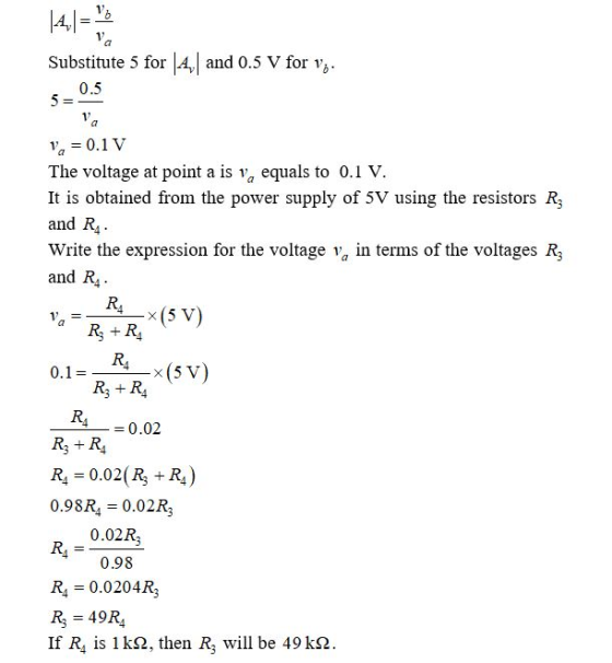
(b) Design the bias input circuit by choosing suitable resistors R3 and R4 such that the voltage vb will be 0.5V if the positive power supply of the op-amp is connected to a 5V battery. Again both switches are open.
(c) Given Sw1 is open, the amplifier is turned on for enough time, such that the voltages stabilise, Michael connects the motor by closing Sw2 and the motor starts to move. Find the step response of the motor current, iout. Assume that the amplifier output resistance is negligible, it does not current limit and the motor inductor has been de-energised.
(d) What is the steady state voltage across the motor?
(e) Perform frequency response analysis from vin, to the voltage across the motor inductor, when both switches are closed and Michael applies three different input signals of 10 Hz, 100 Hz and 1000 Hz through the system?
(f) Plot the response calculated in part (e) in a Bode plot.
(g) Michael realises that his motor can only have a positive voltage and so his robot can only go forwards. If Michael has a second 5V battery, redraw the circuit to allow the motor voltage to vary from +5V to -5V as vin varies from 0V to 3V, respectively. Note that Michael will need to change both the gain and the bias voltage at the non-inverting input.
Please help me do this practice question
Homework Answers


Add Answer to:
(a) Design an inverting amplifier by choosing suitable resistor
values for R1 and R2 to produce...
Mitch is designing a motor driver for a wheeled mobile robot. The motor driver is designed...
 Mitch is designing a motor driver for a wheeled mobile robot.
The motor driver is designed as an inverting amplifier (using the
circuit shown in Figure 1) to drive the motor in the opposite
direction of the input voltage. Mitch would like to select the
components of the amplifier based on specific design requirements.
Mitch has installed a switch
to disconnect the motor driver input signal
to the system and a motor protection switch
to disconnect the motor from the...
Mitch is designing a motor driver for a wheeled mobile robot.
The motor driver is designed as an inverting amplifier (using the
circuit shown in Figure 1) to drive the motor in the opposite
direction of the input voltage. Mitch would like to select the
components of the amplifier based on specific design requirements.
Mitch has installed a switch
to disconnect the motor driver input signal
to the system and a motor protection switch
to disconnect the motor from the...
2. Construct the non-inverting amplifier circuit below. Then, obtain input-output transfer function for R1=1K and R2=2.2K,...
 2. Construct the non-inverting amplifier circuit below. Then, obtain input-output transfer function for R1=1K and R2=2.2K, E= 9V. Use a variable de voltage (5V de source and a variable 1k potentiometer) source as the input and measure the output voltage for different inputs. Draw the input-output transfer function from the measured input-output voltages. Proteus Table Vin Vout Measured Table Vin Vout Q2) Determine the voltage gain VO / Vin of the non-inverting amplifier. What is the output voltage range over...
Inverting Amplifier Figure 4.2 shows the fundamental configuration of Op-Amp in which it is used as...
 Inverting Amplifier Figure 4.2 shows the fundamental configuration of Op-Amp in which it is used as an inverting amplifier. In this configuration the ratio, R2/R1 completely controls the effective gain of the amplifier and it can be verified that the output voltage is equal to Vo = - (R2/R1)Vin R2 100K Q-10V R1 Vinow 20K 1 2 7 V Vo 3 -10v Figure 4.2 Part 1 - Inverting Amp: Procedure 1. Construct the circuit of figure 4.2 using Op-Amp IC...
A. B. 1.Choosing the appropriate one of the two circuits above, design an amplifier that has...
 A.
B.
1.Choosing the appropriate one of the two circuits above, design
an amplifier that has a voltage amplification factor of +10 (i.e.,
the output signal should be 10 times larger than the input signal,
and also be in-phase with the input signal). You may use any values
for your resistors, but avoid values greater than 100 kΩ.
2. construct the circuit using multisim, and perform a transient
analysis
U1 .V43 0.707 Vrms: 60 Hz O° 0PAMP 3T BASIC 2.R1...
A.
B.
1.Choosing the appropriate one of the two circuits above, design
an amplifier that has a voltage amplification factor of +10 (i.e.,
the output signal should be 10 times larger than the input signal,
and also be in-phase with the input signal). You may use any values
for your resistors, but avoid values greater than 100 kΩ.
2. construct the circuit using multisim, and perform a transient
analysis
U1 .V43 0.707 Vrms: 60 Hz O° 0PAMP 3T BASIC 2.R1...
QUESTION 1 Anna the Audiophile has asked for your help to build an amplifier and filter...
 QUESTION 1 Anna the Audiophile has asked for your help to build an amplifier and filter to take small signals from her hifi system and amplify them so that she can drive her new subwoofer. The hifi system produces AC signals at varying frequencies with 250mVrms maximum magnitude Her subwoofer requires the signals to be 20 Vrms maximum magnitude. The signals that Anna is interested in are below 200 Hz. She would like the filter to attenuate signals at frequencies...
Laboratory 1: operation amplifier characteristics A. Objectives: 1. To study the basic characteri...
 thanks
Laboratory 1: operation amplifier characteristics A. Objectives: 1. To study the basic characteristics of an operational amplifier 2. To study the bias circuit of an operational amplifier B. Apparatus: 1. DC Power supply 2. Experimental board and corresponding components 3. Electronic calculator (prepared by students) 4. Digital camera (prepared by students for photo taking of the experimental results) 5. Laptop computer with the software PicoScope 6 and Microsoft Word installed. 6. PicoScope PC Oscilloscope and its accessories. 7. Multimeter...
thanks
Laboratory 1: operation amplifier characteristics A. Objectives: 1. To study the basic characteristics of an operational amplifier 2. To study the bias circuit of an operational amplifier B. Apparatus: 1. DC Power supply 2. Experimental board and corresponding components 3. Electronic calculator (prepared by students) 4. Digital camera (prepared by students for photo taking of the experimental results) 5. Laptop computer with the software PicoScope 6 and Microsoft Word installed. 6. PicoScope PC Oscilloscope and its accessories. 7. Multimeter...
Introduction The purpose of this project is to design, simulate, analyze, implement, and test a single-supply,...
Introduction The purpose of this project is to design, simulate, analyze, implement, and test a single-supply, multistage, transistor amplifier which fulfills a set of specifications. For this project, the pre-lab shall be treated as your formal design report and therefore must be much more detailed than usual (please see Evaluation heading on the next page of this document). The report shall be submitted to the TA by the deadline. The report is an individual assignment. Specifications • Power supply: +???...
A common source amplifier circuit based on a single n-channel MOSFET is shown in Figure 4b. Assume that the transconductance gm-60 mS (equivalent to mA/ V) and drain source resistance, os,...
 A common source amplifier circuit based on a single n-channel MOSFET is shown in Figure 4b. Assume that the transconductance gm-60 mS (equivalent to mA/ V) and drain source resistance, os, is so large it may be neglected. 0) Calculate the open circuit voltage gain Av Yout/ Vis. i) The amplifier has a load of 10 k2. Determine the current gain Va. = 12 V 150k 4k3 Vout Vin 200k GND = 0 V Figure 4b a) State the name...
Problem 3: Design Problem On Figure P3a, you have a Common Source (CS) n-channel MOSFET amplifier....
 Problem 3: Design Problem On Figure P3a, you have a Common Source (CS) n-channel MOSFET amplifier. Notice the absence of a source resistor Rsig and load resistor R. If we know how the present amplifier (the one on Figure P3a) behaves without Rsig and RL, we can infer its behaviors if Rsig and R were to be added. design the amplifier circuit on Figure P3a, i.e., you have to find appropriate values for RGj You are to RG,, RD, and...
Yes, this is one problem. Please solve ALL PARTS. Guaranteed thumbs up for the person who solves it. 3 1. Photodiode...
 Yes, this is one problem. Please solve ALL PARTS. Guaranteed
thumbs up for the person who solves it.
3 1. Photodiode amplifier circuit You are designinga CF photosensor circuit for a light detection and ranging LiDAR) system in autonomous vehicles. The circuit utilizes a transimpedance amplifier to convert low-level RF photodiode current signal to a usable voltage output. It consists of a photodiode, an amplifier, and feedback capacitor/resistor pair as shown in Figure 1. We will derive simple equations to...
Yes, this is one problem. Please solve ALL PARTS. Guaranteed
thumbs up for the person who solves it.
3 1. Photodiode amplifier circuit You are designinga CF photosensor circuit for a light detection and ranging LiDAR) system in autonomous vehicles. The circuit utilizes a transimpedance amplifier to convert low-level RF photodiode current signal to a usable voltage output. It consists of a photodiode, an amplifier, and feedback capacitor/resistor pair as shown in Figure 1. We will derive simple equations to...
 Mitch is designing a motor driver for a wheeled mobile robot.
The motor driver is designed as an inverting amplifier (using the
circuit shown in Figure 1) to drive the motor in the opposite
direction of the input voltage. Mitch would like to select the
components of the amplifier based on specific design requirements.
Mitch has installed a switch
to disconnect the motor driver input signal
to the system and a motor protection switch
to disconnect the motor from the...
Mitch is designing a motor driver for a wheeled mobile robot.
The motor driver is designed as an inverting amplifier (using the
circuit shown in Figure 1) to drive the motor in the opposite
direction of the input voltage. Mitch would like to select the
components of the amplifier based on specific design requirements.
Mitch has installed a switch
to disconnect the motor driver input signal
to the system and a motor protection switch
to disconnect the motor from the...
 2. Construct the non-inverting amplifier circuit below. Then, obtain input-output transfer function for R1=1K and R2=2.2K, E= 9V. Use a variable de voltage (5V de source and a variable 1k potentiometer) source as the input and measure the output voltage for different inputs. Draw the input-output transfer function from the measured input-output voltages. Proteus Table Vin Vout Measured Table Vin Vout Q2) Determine the voltage gain VO / Vin of the non-inverting amplifier. What is the output voltage range over...
 Inverting Amplifier Figure 4.2 shows the fundamental configuration of Op-Amp in which it is used as an inverting amplifier. In this configuration the ratio, R2/R1 completely controls the effective gain of the amplifier and it can be verified that the output voltage is equal to Vo = - (R2/R1)Vin R2 100K Q-10V R1 Vinow 20K 1 2 7 V Vo 3 -10v Figure 4.2 Part 1 - Inverting Amp: Procedure 1. Construct the circuit of figure 4.2 using Op-Amp IC...
 A.
B.
1.Choosing the appropriate one of the two circuits above, design
an amplifier that has a voltage amplification factor of +10 (i.e.,
the output signal should be 10 times larger than the input signal,
and also be in-phase with the input signal). You may use any values
for your resistors, but avoid values greater than 100 kΩ.
2. construct the circuit using multisim, and perform a transient
analysis
U1 .V43 0.707 Vrms: 60 Hz O° 0PAMP 3T BASIC 2.R1...
A.
B.
1.Choosing the appropriate one of the two circuits above, design
an amplifier that has a voltage amplification factor of +10 (i.e.,
the output signal should be 10 times larger than the input signal,
and also be in-phase with the input signal). You may use any values
for your resistors, but avoid values greater than 100 kΩ.
2. construct the circuit using multisim, and perform a transient
analysis
U1 .V43 0.707 Vrms: 60 Hz O° 0PAMP 3T BASIC 2.R1...
 QUESTION 1 Anna the Audiophile has asked for your help to build an amplifier and filter to take small signals from her hifi system and amplify them so that she can drive her new subwoofer. The hifi system produces AC signals at varying frequencies with 250mVrms maximum magnitude Her subwoofer requires the signals to be 20 Vrms maximum magnitude. The signals that Anna is interested in are below 200 Hz. She would like the filter to attenuate signals at frequencies...
 thanks
Laboratory 1: operation amplifier characteristics A. Objectives: 1. To study the basic characteristics of an operational amplifier 2. To study the bias circuit of an operational amplifier B. Apparatus: 1. DC Power supply 2. Experimental board and corresponding components 3. Electronic calculator (prepared by students) 4. Digital camera (prepared by students for photo taking of the experimental results) 5. Laptop computer with the software PicoScope 6 and Microsoft Word installed. 6. PicoScope PC Oscilloscope and its accessories. 7. Multimeter...
thanks
Laboratory 1: operation amplifier characteristics A. Objectives: 1. To study the basic characteristics of an operational amplifier 2. To study the bias circuit of an operational amplifier B. Apparatus: 1. DC Power supply 2. Experimental board and corresponding components 3. Electronic calculator (prepared by students) 4. Digital camera (prepared by students for photo taking of the experimental results) 5. Laptop computer with the software PicoScope 6 and Microsoft Word installed. 6. PicoScope PC Oscilloscope and its accessories. 7. Multimeter...
 A common source amplifier circuit based on a single n-channel MOSFET is shown in Figure 4b. Assume that the transconductance gm-60 mS (equivalent to mA/ V) and drain source resistance, os, is so large it may be neglected. 0) Calculate the open circuit voltage gain Av Yout/ Vis. i) The amplifier has a load of 10 k2. Determine the current gain Va. = 12 V 150k 4k3 Vout Vin 200k GND = 0 V Figure 4b a) State the name...
 Problem 3: Design Problem On Figure P3a, you have a Common Source (CS) n-channel MOSFET amplifier. Notice the absence of a source resistor Rsig and load resistor R. If we know how the present amplifier (the one on Figure P3a) behaves without Rsig and RL, we can infer its behaviors if Rsig and R were to be added. design the amplifier circuit on Figure P3a, i.e., you have to find appropriate values for RGj You are to RG,, RD, and...
 Yes, this is one problem. Please solve ALL PARTS. Guaranteed
thumbs up for the person who solves it.
3 1. Photodiode amplifier circuit You are designinga CF photosensor circuit for a light detection and ranging LiDAR) system in autonomous vehicles. The circuit utilizes a transimpedance amplifier to convert low-level RF photodiode current signal to a usable voltage output. It consists of a photodiode, an amplifier, and feedback capacitor/resistor pair as shown in Figure 1. We will derive simple equations to...
Yes, this is one problem. Please solve ALL PARTS. Guaranteed
thumbs up for the person who solves it.
3 1. Photodiode amplifier circuit You are designinga CF photosensor circuit for a light detection and ranging LiDAR) system in autonomous vehicles. The circuit utilizes a transimpedance amplifier to convert low-level RF photodiode current signal to a usable voltage output. It consists of a photodiode, an amplifier, and feedback capacitor/resistor pair as shown in Figure 1. We will derive simple equations to...
Most questions answered within 3 hours.
-
Jamie is doing a survey at her school about whether the students
feel the cafeteria food...
asked 52 minutes ago -
How many liters of 0.669 M KOH will be needed to raise the pH of
0.339...
asked 3 hours ago -
A liquid of density 1270 kg/m 3 flows steadily through a pipe of
varying diameter and...
asked 3 hours ago -
Questions: What should the American executive do?
'A visiting American executive finds that a foreign subsidiary...
asked 3 hours ago -
Activity based costing was introduced as an alternative to
absorption costing.
1. Discuss using illustration the...
asked 3 hours ago -
1. You own shares of Crane DVD Company and are interested in
selling them. With so...
asked 3 hours ago -
How many grams of He are necessary to fill a balloon having a
volume of 4.5E3...
asked 3 hours ago -
The 2 patients, still in the hospital, were interviewed by a
MoH epidemiologist. The interviews revealed...
asked 3 hours ago -
An uncharged capacitor and a resistor are connected in series to
a source of emf. If...
asked 3 hours ago -
If assets are $540,000 and liabilities are $236,000 what is the
amount of owner’s equity?
asked 3 hours ago -
MATH 3421 Maple Assignment 1 Due February 13, 2019 Maple is a
Computer Algebra System that...
asked 3 hours ago -
CODING IN JAVA
Dates are printed in several common formats. Two of the more
common formats...
asked 3 hours ago