For an indirect gap semiconductor such as silicon, the difference in wave vector between the VBM...
For an indirect gap semiconductor such as silicon, the
difference
in wave vector between the VBM and the CBM is on the order of ?k =
?∕a, where a is the lattice constant of the material. (a) Explain
why this
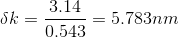
is so. (b) Estimate ?k for Si, where the lattice constant is 0.543
nm. (c) For
an optical transition to take place, the photon needs to have at
least the gap
energy (1.11 eV for Si) and it has to have a wave vector
corresponding to ?k.
What is the actual size of the wave vector of 1.11 eV photons? For
which type
of electromagnetic radiation does the modulus of the wave vector
become
comparable to the reciprocal lattice distances in a solid?
Homework Answers
a) We know that for an indirect semiconductor like Si, the photon can not be emitted directly as the transition between the Conduction band and Valence band can not take place directly but passes through an intermediate state by transferring the momentum through the crystal lattice,, having lattice spacing a. The process needs to be take place in such a manner that the energy and momentum conservation must hold . The study of Brillouin zone revealed that the wavevector of the electron in a crystal lattice is ranging from -pi/a to +pi/a. So when an electron recombines with a hole in the valence band, the difference in momentum transfers to the lattice leading to change in momentum delta k as

It met the condition of interference.
(b) Putting the value of a in above we get
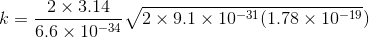
(b) The energy E can be given as


Solving for k and treating ko as reference level.

The actual wave vector will be 5.42nm.
(c) The corresponding wavelength lambda becomes

It represents the X-ray module system
Add Answer to:
For an indirect gap semiconductor such as silicon, the
difference
in wave vector between the VBM...
QUESTION 9 If a semiconductor with a larger bandgap than Si is used in a single...
 QUESTION 9 If a semiconductor with a larger bandgap than Si is used in a single junction photovoltaic cell, which of the following (may be more than one) will be true? The efficiency of the cell will increase. The cell will be less effective at converting IR radiation from the sun to electricity. The semiconductor will not require doping. The cell will be more effective at converting higher energy solar photons (corresponding to its band gap) to electricity. QUESTION 10...
Theory section is below for the equations PRELAB Read the theory section below. Calculate the photon...
 Theory section is below for the equations
PRELAB Read the theory section below. Calculate the photon wavelength in nm corresponding to a photon energy equal to the theoretical band gap energy of S1.121 eV and GaAs, 1.422 eV. These will be used to set the monochromator. THEORY One of the most important characteristics of a semiconductor is its band gap energy Eg Whereas an electron in an isolated atom has discrete energy levels, an electron in a semiconductor crystal has...
Theory section is below for the equations
PRELAB Read the theory section below. Calculate the photon wavelength in nm corresponding to a photon energy equal to the theoretical band gap energy of S1.121 eV and GaAs, 1.422 eV. These will be used to set the monochromator. THEORY One of the most important characteristics of a semiconductor is its band gap energy Eg Whereas an electron in an isolated atom has discrete energy levels, an electron in a semiconductor crystal has...
 QUESTION 9 If a semiconductor with a larger bandgap than Si is used in a single junction photovoltaic cell, which of the following (may be more than one) will be true? The efficiency of the cell will increase. The cell will be less effective at converting IR radiation from the sun to electricity. The semiconductor will not require doping. The cell will be more effective at converting higher energy solar photons (corresponding to its band gap) to electricity. QUESTION 10...
 Theory section is below for the equations
PRELAB Read the theory section below. Calculate the photon wavelength in nm corresponding to a photon energy equal to the theoretical band gap energy of S1.121 eV and GaAs, 1.422 eV. These will be used to set the monochromator. THEORY One of the most important characteristics of a semiconductor is its band gap energy Eg Whereas an electron in an isolated atom has discrete energy levels, an electron in a semiconductor crystal has...
Theory section is below for the equations
PRELAB Read the theory section below. Calculate the photon wavelength in nm corresponding to a photon energy equal to the theoretical band gap energy of S1.121 eV and GaAs, 1.422 eV. These will be used to set the monochromator. THEORY One of the most important characteristics of a semiconductor is its band gap energy Eg Whereas an electron in an isolated atom has discrete energy levels, an electron in a semiconductor crystal has...
Most questions answered within 3 hours.
-
A hospital performs 100 surgeries per week. The probability that
complications after surgery occur is 10%....
asked 20 seconds ago -
A 5.20 mW helium neon laser emits a visible laser beam with a
wavelength of 633...
asked 54 seconds ago -
In preparing its cash flow statement for the year ended December
31, 2018, Green Co. gathered...
asked 2 minutes ago -
Donna is 18 years old and full time accounting student.She is
saving for an overseas holiday...
asked 2 minutes ago -
Service-oriented architectures (SOA) provide
object-oriented architectures for web platforms that represent a
collection of services. SOA...
asked 3 minutes ago -
Le Terroir Winery is considering an expansion project to produce
fine wines. The trial expansion will...
asked 12 minutes ago -
The Bahraini public budget experiences deficit in the last
seven years, what are procedures are taken...
asked 19 minutes ago -
You invested $30,000 in a mutual fund at the beginning of the
year when the NAV...
asked 22 minutes ago -
Would you expect the price elasticity of supply for guitars to
be more inelastic in the...
asked 24 minutes ago -
A snowmobile is originally at the point with position vector
30.1 m at 95.0° counterclockwise from...
asked 24 minutes ago -
MAN3240 Organizational Behavior
In one to two paragraphs
6.) How can understanding emotions make me more...
asked 32 minutes ago -
Identify one individual who, in your opinion, is an excellent
leader. List the qualities that this...
asked 30 minutes ago