
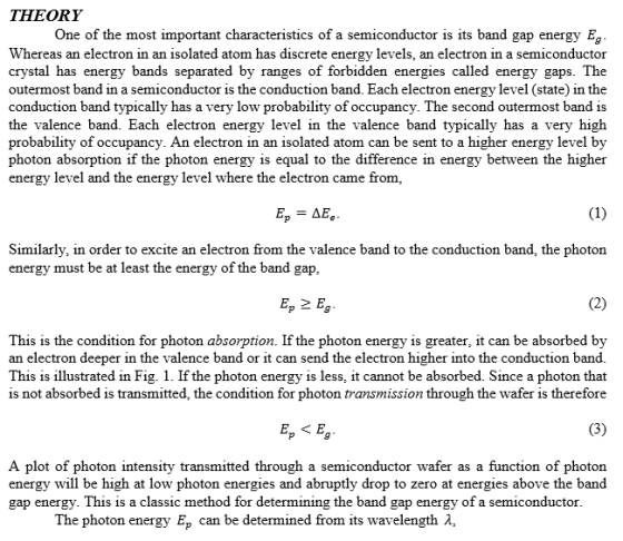
Theory section is below for the equations
Homework Answers

Add Answer to:
Theory section is below for the equations
PRELAB Read the theory section below. Calculate the photon...
4. A photon of light can excite an electron from the valence band to the conduction...
 4. A photon of light can excite an electron from the valence band to the conduction band of a semiconductor. This process is called photoconduction. a. PbS has a band gap of 0.37 eV. What wavelength of light would be needed to start the photoconduction in this semiconductor? b. In the light meters of cameras one would need a semiconductor that operates efficiently in visible light, or at-550 nm. Would PbS be a suitable semiconductor for a light meter? Why...
(2) In a semiconductor with an energy gap Eg between the valence and the conduction bands we can take Ef (the Fermi ene...
 (2) In a semiconductor with an energy gap Eg between the valence and the conduction bands we can take Ef (the Fermi energy) to be halfway between the bands (see figure below): Conduction band Energy gap Eg Valence band Semiconductor a. Show that for a typical semiconductor or insulator at room temperature the Fermi- Dirac factor is approximately equal to exp(-E 2kBT). (Typical Eg for semi-conductors ranges from about 0.5eV to 6eV at T-293K.) b. In heavily doped n-type silicon,...
The energy gap for a semiconductor is 1.25 eV. Of the frequencies given below, what is...
The energy gap for a semiconductor is 1.25 eV. Of the frequencies given below, what is the minimum frequency photon than can move an electron from the valence band to the conduction band?
3. The figure below shows a schematic of the dispersion for the conduction and valence bands...
 3. The figure below shows a schematic of the dispersion for the conduction and valence bands for particular semiconductor. The conduction band has dispersion equation a 10-35 E (3 x 10 19) [2 x 10 and the valence band has dispersion equation E (4 x 10-37A2 where in both cases E is in units of joules and k in units of m1 E 6x 10-19 J 2 6 x 10 m -6 -4 -2 2 k (a) Is this a...
3. Many parameters of crystals are dependent on the band gap. a) From the optical absorption...
 3. Many parameters of crystals are dependent on the band gap. a) From the optical absorption spectrum of a certain semiconductor, one finds that the longest wavelength of radiation absorbed is 1.40 m. What is the band gap for this semiconductor? Explain how the band gap gives rise to this behavior. b) What band gap would be needed to make blue (450 nm) LEDs? Explain why. c) Most of the sun's radiation has wavelengths shorter than 1000 nm. For a...
The gap between valence and conduction bands in silicon is 1.12 eV. A nickel nucleus in...
The gap between valence and conduction bands in silicon is 1.12 eV. A nickel nucleus in an excited state emits a photon with wavelength 5.87x10⁻⁴ nm. How many electrons can be excited from the top of the valence band to the bottom of the conduction band by the absorption of this gamma ray? Provide your answer in mega electrons (mega x106).
Band structure Consider a one-dimensional semiconductor crystal consisting of 11 atoms with nearest- neighbor atoms separated...
 Band structure Consider a one-dimensional semiconductor crystal consisting of 11 atoms with nearest- neighbor atoms separated by a 5 . The band structure for electrons in the conduction band is given by Ec(k) = 101(k-0.2n)2-A(k-02n)"] + 2.25 [eV] and the band structure for holes in the valence band is given by where the wavevector k s in units ofA-1. The allowed wavevectors are--< k 즈 al (a) Is this a direct or indirect gap semiconductor? What is the energy gap...
Experiment 11: Investigating Bandgap Energies, Materials, and Design of Light-Emitting Diodes (LED) 3. For a device...
 Experiment 11: Investigating Bandgap Energies, Materials, and Design of Light-Emitting Diodes (LED) 3. For a device to be a good conductor, there must be a significant electron population in the conduction band. When no energy is supplied to a semiconductor, the relative population of the conduction band follows Boltzmann's population law. In the case of a diode, the equation is: CB Population = e /RT VB Population Where CB and VB population are the respective electron populations in the conduc-...
PART A: The electrons in solids can be found ____________in only certain discrete sharp energy states...
PART A: The electrons in solids can be found ____________in only certain discrete sharp energy states associated with their orbits.in energy states that overlap so that more than one electron is associated with a given energy level.in the same energy states as if the atoms forming the solid were far enough so that their interactions could be neglected.in closely spaced energy levels that form a continuous distribution of energy within a certain range.PART B: When an electron in the valence...
 4. A photon of light can excite an electron from the valence band to the conduction band of a semiconductor. This process is called photoconduction. a. PbS has a band gap of 0.37 eV. What wavelength of light would be needed to start the photoconduction in this semiconductor? b. In the light meters of cameras one would need a semiconductor that operates efficiently in visible light, or at-550 nm. Would PbS be a suitable semiconductor for a light meter? Why...
 4. A photon of light can excite an electron from the valence band to the conduction band of a semiconductor. This process is called photoconduction. a. PbS has a band gap of 0.37 eV. What wavelength of light would be needed to start the photoconduction in this semiconductor? b. In the light meters of cameras one would need a semiconductor that operates efficiently in visible light, or at-550 nm. Would PbS be a suitable semiconductor for a light meter? Why...
 (2) In a semiconductor with an energy gap Eg between the valence and the conduction bands we can take Ef (the Fermi energy) to be halfway between the bands (see figure below): Conduction band Energy gap Eg Valence band Semiconductor a. Show that for a typical semiconductor or insulator at room temperature the Fermi- Dirac factor is approximately equal to exp(-E 2kBT). (Typical Eg for semi-conductors ranges from about 0.5eV to 6eV at T-293K.) b. In heavily doped n-type silicon,...
 3. The figure below shows a schematic of the dispersion for the conduction and valence bands for particular semiconductor. The conduction band has dispersion equation a 10-35 E (3 x 10 19) [2 x 10 and the valence band has dispersion equation E (4 x 10-37A2 where in both cases E is in units of joules and k in units of m1 E 6x 10-19 J 2 6 x 10 m -6 -4 -2 2 k (a) Is this a...
 3. Many parameters of crystals are dependent on the band gap. a) From the optical absorption spectrum of a certain semiconductor, one finds that the longest wavelength of radiation absorbed is 1.40 m. What is the band gap for this semiconductor? Explain how the band gap gives rise to this behavior. b) What band gap would be needed to make blue (450 nm) LEDs? Explain why. c) Most of the sun's radiation has wavelengths shorter than 1000 nm. For a...
 Band structure Consider a one-dimensional semiconductor crystal consisting of 11 atoms with nearest- neighbor atoms separated by a 5 . The band structure for electrons in the conduction band is given by Ec(k) = 101(k-0.2n)2-A(k-02n)"] + 2.25 [eV] and the band structure for holes in the valence band is given by where the wavevector k s in units ofA-1. The allowed wavevectors are--< k 즈 al (a) Is this a direct or indirect gap semiconductor? What is the energy gap...
 Experiment 11: Investigating Bandgap Energies, Materials, and Design of Light-Emitting Diodes (LED) 3. For a device to be a good conductor, there must be a significant electron population in the conduction band. When no energy is supplied to a semiconductor, the relative population of the conduction band follows Boltzmann's population law. In the case of a diode, the equation is: CB Population = e /RT VB Population Where CB and VB population are the respective electron populations in the conduc-...
Most questions answered within 3 hours.
-
A 12.87-g block of solid iron
at 68.39 °C is immersed in a
21.10-g pool of...
asked 50 seconds ago -
What is happening molecularly that causes primers to not bind as
well at high temperatures?
asked 2 minutes ago -
In the movie You've Got Mail, what key concepts of gendered
communication could be related to...
asked 5 minutes ago -
Hello, Any help on these questions would be greatly
appreciated.
1. In a perfectly competitive market,...
asked 5 minutes ago -
You are working with Drosophila, and cross females from a
true-breeding strain with white
eyes to...
asked 6 minutes ago -
Using Python programming, create a 2-by-3 list, then use a
nested loop to:
1) Set each...
asked 40 minutes ago -
You are investigating an arson scene and you find a corpse in
the rubble, but you...
asked 56 minutes ago -
Do you agree with Hegel that human history exhibits progress?
Does human history exhibit the kind...
asked 1 hour ago -
1. Ashton Company began the year with a zero balance in its
Supplies General Ledger account....
asked 58 minutes ago -
Can someone help me please:
Discuss Facebook's policies from a privacy perspective. What
does it do...
asked 57 minutes ago -
Like a good economist, you calculated the opportunity cost of
getting your college degree. Suppose that...
asked 1 hour ago -
A 1500 kg car drives around a flat circular track at a constant
speed of 75...
asked 1 hour ago