
Homework Answers


Add Answer to:
Question 4 The input signal to the circuit below is a Triangle wave with a peak...
Question 13 The input Vs to the comparator circuit below is a 10 V Triangle Wave....
 Question 13 The input Vs to the comparator circuit below is a 10 V Triangle Wave. Determine the voltage Vs when the output of the comparator will become maximum positive VCC = 12 V, R1 10 k2, R2 = 3.1 k Enter your results in volts. Do not type the units Vcc R1 Vout R2 AN Vs ww
Question 13 The input Vs to the comparator circuit below is a 10 V Triangle Wave. Determine the voltage Vs when the...
Question 13 The input Vs to the comparator circuit below is a 10 V Triangle Wave. Determine the voltage Vs when the output of the comparator will become maximum positive VCC = 12 V, R1 10 k2, R2 = 3.1 k Enter your results in volts. Do not type the units Vcc R1 Vout R2 AN Vs ww
Question 13 The input Vs to the comparator circuit below is a 10 V Triangle Wave. Determine the voltage Vs when the...
PROTEUS +15V R5 1M R3 750 C3 HE Dvout luf Q1 ZVN2110 R1 C1 R4 100F...
 PROTEUS
+15V R5 1M R3 750 C3 HE Dvout luf Q1 ZVN2110 R1 C1 R4 100F V1 VSINE R6 1M R2 1k C2 Tur Figure 8.2. CS Amplifier with a bypassed Rs 1. Design and build the common source amplifier as shown in Figure 8.2. 2. Provide Vai= 100 m Vpp at 5 KHz frequency and measure the output voltage. 3. Record pictures of the input and output waveforms and calculate the gain. 4. Vary Vsig (Try 1V, 400mV, 100mV)...
PROTEUS
+15V R5 1M R3 750 C3 HE Dvout luf Q1 ZVN2110 R1 C1 R4 100F V1 VSINE R6 1M R2 1k C2 Tur Figure 8.2. CS Amplifier with a bypassed Rs 1. Design and build the common source amplifier as shown in Figure 8.2. 2. Provide Vai= 100 m Vpp at 5 KHz frequency and measure the output voltage. 3. Record pictures of the input and output waveforms and calculate the gain. 4. Vary Vsig (Try 1V, 400mV, 100mV)...
1. For the 4 circuits shown below, sketch the output waveform for a 1V peak, 1kHz,...
 1. For the 4 circuits shown below, sketch the output waveform for a 1V peak, 1kHz, sinusoidal wave in put signal. Assume the diodes are ideal and they exhibit ON-OFF switch model behaviour. Create an ideal diode model in LT-Spice with the following specification [.model IdealDiode D(Ron=0.1m Roff=100G Vfwd-0.0) ] simulate the circuit and verify the output waveform. Vin Vout Vin Vout 1k 1k (a) (b) 1k Vin 1k Vin Vout Vout ww 1k (c) (d) KH
1. For the...
1. For the 4 circuits shown below, sketch the output waveform for a 1V peak, 1kHz, sinusoidal wave in put signal. Assume the diodes are ideal and they exhibit ON-OFF switch model behaviour. Create an ideal diode model in LT-Spice with the following specification [.model IdealDiode D(Ron=0.1m Roff=100G Vfwd-0.0) ] simulate the circuit and verify the output waveform. Vin Vout Vin Vout 1k 1k (a) (b) 1k Vin 1k Vin Vout Vout ww 1k (c) (d) KH
1. For the...
w R Vinn Vou V. R W (a) (b) An alternating square wave signal f(t) has...
 w R Vinn Vou V. R W (a) (b) An alternating square wave signal f(t) has frequency, f = 1 kHz, peak-to-peak voltage, Vpp = 8 V and zero DC offset. (10 pts) A. Given that Vin(t) = f(t), find the steady-state output voltage value for Circuit (a) when i. Vin(t) > 0; ii. Vin(t) <0. B. Given that Vin(t) = f(t), find the steady-state output voltage value for Circuit (b) when i. Vin(t)>0; ii. Vin(t) <0. C. Given that...
(a) Design a inverting Schmitt trigger circuit to be used as a zero crossing detector with transition voltages about ±25...
 (a) Design a inverting Schmitt trigger circuit
to be used as a zero crossing detector with transition voltages
about ±25 mV. Assume the saturation voltages for the op–amp are ±13
V. Draw the voltage transfer characteristic (VTC), i.e., vout vs.
vin.
(b) Design an astable multivibrator to produce
a square signal with a frequency of 1 kHz using C=0.01 µF, R1 = 30
kΩ, and R2 = 20 kΩ. Sketch the circuit waveforms (vo, v +, and v −)
assuming...
(a) Design a inverting Schmitt trigger circuit
to be used as a zero crossing detector with transition voltages
about ±25 mV. Assume the saturation voltages for the op–amp are ±13
V. Draw the voltage transfer characteristic (VTC), i.e., vout vs.
vin.
(b) Design an astable multivibrator to produce
a square signal with a frequency of 1 kHz using C=0.01 µF, R1 = 30
kΩ, and R2 = 20 kΩ. Sketch the circuit waveforms (vo, v +, and v −)
assuming...
A MOSFET is wired as a common-source amplifier as shown below. The input voltage vIN is...
 A MOSFET is wired as a common-source amplifier as shown below.
The input voltage vIN is the total of the source for
biasing the circuit at its operating point (vBIAS), and
a small signal ac source providing the signal that we want to
amplify (vin). The total output voltage is
vO.
a) Assume VDD = 5?, VIN = 2?, and ? = 4?Ω
in the circuit and the MOSFET parameters are K =
0.5??/?2, VTH 1?, and ? = 0.05V-1....
A MOSFET is wired as a common-source amplifier as shown below.
The input voltage vIN is the total of the source for
biasing the circuit at its operating point (vBIAS), and
a small signal ac source providing the signal that we want to
amplify (vin). The total output voltage is
vO.
a) Assume VDD = 5?, VIN = 2?, and ? = 4?Ω
in the circuit and the MOSFET parameters are K =
0.5??/?2, VTH 1?, and ? = 0.05V-1....
In the circuit of given below, Vsig is a small sine wave signal with zero average. The transistor...
 In the circuit of given below, Vsig is a small sine wave signal with zero average. The transistor B is 100. a) Find the value of RE to establish a dc emitter current of about 0.5 mA. b) Find Rc to establish a dc collector voltage of about +5 V c) For RL10 kS2 and the transistor ro 200 k2, draw the small-signal equivalent circuit 5. of the amplifier and determine its overall voltage gain +15 V Re O Vo...
Lab ll: Voltage Follower ECE 210: 1. For the following circuit, Theoretically calculate the peak ...
 URGENT!! PLEASE HELP! be clear and answer all questions
clearly!!
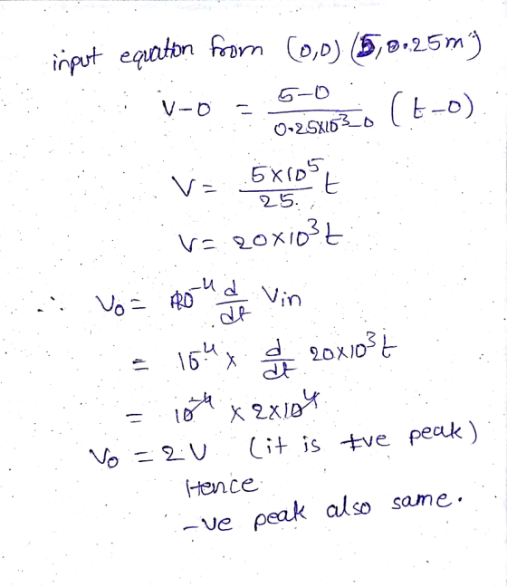
Lab ll: Voltage Follower ECE 210: 1. For the following circuit, Theoretically calculate the peak voltage across R3 (Vo) an ved R1-2.2k0 2.17362(Actual) R2 = 3.3kN-3.Z44KAL (Actual) R3-10kΩ 9.873M. (Actual) Vin- 1kHz Triangle wave, 2V peak, NO DC offset e) R Draw the output waveform Vo: UI R1 R2 X-Axis 0.1 msec/div 2. Remove the resistor R2 to create the following circuit Draw the output waveform Vo: U1 R1 R3...
URGENT!! PLEASE HELP! be clear and answer all questions
clearly!!
Lab ll: Voltage Follower ECE 210: 1. For the following circuit, Theoretically calculate the peak voltage across R3 (Vo) an ved R1-2.2k0 2.17362(Actual) R2 = 3.3kN-3.Z44KAL (Actual) R3-10kΩ 9.873M. (Actual) Vin- 1kHz Triangle wave, 2V peak, NO DC offset e) R Draw the output waveform Vo: UI R1 R2 X-Axis 0.1 msec/div 2. Remove the resistor R2 to create the following circuit Draw the output waveform Vo: U1 R1 R3...
The circuit 3-The circuit of problem # 2 is subjected to a small ac input by the signal generator. By neglecting the voltage drop across the coupling and bypass capacitors, determine the small signa...
 The circuit
3-The circuit of problem # 2 is subjected to a small ac input by the signal generator. By neglecting the voltage drop across the coupling and bypass capacitors, determine the small signal voltage gain Vo/ Vì = Avi , input resistance Ri-vi / ii and the output resistance Ro external to R Avi= Ri= , Ro The accompanying circuit shows a 4-resistor biased JFET transistor Determine the values of Rp and Rs so that the Q-point is equal...
The circuit
3-The circuit of problem # 2 is subjected to a small ac input by the signal generator. By neglecting the voltage drop across the coupling and bypass capacitors, determine the small signal voltage gain Vo/ Vì = Avi , input resistance Ri-vi / ii and the output resistance Ro external to R Avi= Ri= , Ro The accompanying circuit shows a 4-resistor biased JFET transistor Determine the values of Rp and Rs so that the Q-point is equal...
IV, Laboratory Procedure 1. Construct the circuit of Figure 6.1, measure the current value 2. Con...
 IV, Laboratory Procedure 1. Construct the circuit of Figure 6.1, measure the current value 2. Construct the circuit of Figure 6.2; measure Vn and v., using the oscilloscope. 3. Construct the circuit of Figure 6.3, measure the value of Io and V 4. Construct the clipper design circuit, Capture the input and output waveforms. 5. Construct your clamper design circuit. Capture the input and output waveforms Figure 6.3 Design a clipper circuit which limits input signals to +3V and -2V....
 Question 13 The input Vs to the comparator circuit below is a 10 V Triangle Wave. Determine the voltage Vs when the output of the comparator will become maximum positive VCC = 12 V, R1 10 k2, R2 = 3.1 k Enter your results in volts. Do not type the units Vcc R1 Vout R2 AN Vs ww
Question 13 The input Vs to the comparator circuit below is a 10 V Triangle Wave. Determine the voltage Vs when the...
Question 13 The input Vs to the comparator circuit below is a 10 V Triangle Wave. Determine the voltage Vs when the output of the comparator will become maximum positive VCC = 12 V, R1 10 k2, R2 = 3.1 k Enter your results in volts. Do not type the units Vcc R1 Vout R2 AN Vs ww
Question 13 The input Vs to the comparator circuit below is a 10 V Triangle Wave. Determine the voltage Vs when the...
 PROTEUS
+15V R5 1M R3 750 C3 HE Dvout luf Q1 ZVN2110 R1 C1 R4 100F V1 VSINE R6 1M R2 1k C2 Tur Figure 8.2. CS Amplifier with a bypassed Rs 1. Design and build the common source amplifier as shown in Figure 8.2. 2. Provide Vai= 100 m Vpp at 5 KHz frequency and measure the output voltage. 3. Record pictures of the input and output waveforms and calculate the gain. 4. Vary Vsig (Try 1V, 400mV, 100mV)...
PROTEUS
+15V R5 1M R3 750 C3 HE Dvout luf Q1 ZVN2110 R1 C1 R4 100F V1 VSINE R6 1M R2 1k C2 Tur Figure 8.2. CS Amplifier with a bypassed Rs 1. Design and build the common source amplifier as shown in Figure 8.2. 2. Provide Vai= 100 m Vpp at 5 KHz frequency and measure the output voltage. 3. Record pictures of the input and output waveforms and calculate the gain. 4. Vary Vsig (Try 1V, 400mV, 100mV)...
 1. For the 4 circuits shown below, sketch the output waveform for a 1V peak, 1kHz, sinusoidal wave in put signal. Assume the diodes are ideal and they exhibit ON-OFF switch model behaviour. Create an ideal diode model in LT-Spice with the following specification [.model IdealDiode D(Ron=0.1m Roff=100G Vfwd-0.0) ] simulate the circuit and verify the output waveform. Vin Vout Vin Vout 1k 1k (a) (b) 1k Vin 1k Vin Vout Vout ww 1k (c) (d) KH
1. For the...
1. For the 4 circuits shown below, sketch the output waveform for a 1V peak, 1kHz, sinusoidal wave in put signal. Assume the diodes are ideal and they exhibit ON-OFF switch model behaviour. Create an ideal diode model in LT-Spice with the following specification [.model IdealDiode D(Ron=0.1m Roff=100G Vfwd-0.0) ] simulate the circuit and verify the output waveform. Vin Vout Vin Vout 1k 1k (a) (b) 1k Vin 1k Vin Vout Vout ww 1k (c) (d) KH
1. For the...
 w R Vinn Vou V. R W (a) (b) An alternating square wave signal f(t) has frequency, f = 1 kHz, peak-to-peak voltage, Vpp = 8 V and zero DC offset. (10 pts) A. Given that Vin(t) = f(t), find the steady-state output voltage value for Circuit (a) when i. Vin(t) > 0; ii. Vin(t) <0. B. Given that Vin(t) = f(t), find the steady-state output voltage value for Circuit (b) when i. Vin(t)>0; ii. Vin(t) <0. C. Given that...
 (a) Design a inverting Schmitt trigger circuit
to be used as a zero crossing detector with transition voltages
about ±25 mV. Assume the saturation voltages for the op–amp are ±13
V. Draw the voltage transfer characteristic (VTC), i.e., vout vs.
vin.
(b) Design an astable multivibrator to produce
a square signal with a frequency of 1 kHz using C=0.01 µF, R1 = 30
kΩ, and R2 = 20 kΩ. Sketch the circuit waveforms (vo, v +, and v −)
assuming...
(a) Design a inverting Schmitt trigger circuit
to be used as a zero crossing detector with transition voltages
about ±25 mV. Assume the saturation voltages for the op–amp are ±13
V. Draw the voltage transfer characteristic (VTC), i.e., vout vs.
vin.
(b) Design an astable multivibrator to produce
a square signal with a frequency of 1 kHz using C=0.01 µF, R1 = 30
kΩ, and R2 = 20 kΩ. Sketch the circuit waveforms (vo, v +, and v −)
assuming...
 A MOSFET is wired as a common-source amplifier as shown below.
The input voltage vIN is the total of the source for
biasing the circuit at its operating point (vBIAS), and
a small signal ac source providing the signal that we want to
amplify (vin). The total output voltage is
vO.
a) Assume VDD = 5?, VIN = 2?, and ? = 4?Ω
in the circuit and the MOSFET parameters are K =
0.5??/?2, VTH 1?, and ? = 0.05V-1....
A MOSFET is wired as a common-source amplifier as shown below.
The input voltage vIN is the total of the source for
biasing the circuit at its operating point (vBIAS), and
a small signal ac source providing the signal that we want to
amplify (vin). The total output voltage is
vO.
a) Assume VDD = 5?, VIN = 2?, and ? = 4?Ω
in the circuit and the MOSFET parameters are K =
0.5??/?2, VTH 1?, and ? = 0.05V-1....
 In the circuit of given below, Vsig is a small sine wave signal with zero average. The transistor B is 100. a) Find the value of RE to establish a dc emitter current of about 0.5 mA. b) Find Rc to establish a dc collector voltage of about +5 V c) For RL10 kS2 and the transistor ro 200 k2, draw the small-signal equivalent circuit 5. of the amplifier and determine its overall voltage gain +15 V Re O Vo...
 URGENT!! PLEASE HELP! be clear and answer all questions
clearly!!
Lab ll: Voltage Follower ECE 210: 1. For the following circuit, Theoretically calculate the peak voltage across R3 (Vo) an ved R1-2.2k0 2.17362(Actual) R2 = 3.3kN-3.Z44KAL (Actual) R3-10kΩ 9.873M. (Actual) Vin- 1kHz Triangle wave, 2V peak, NO DC offset e) R Draw the output waveform Vo: UI R1 R2 X-Axis 0.1 msec/div 2. Remove the resistor R2 to create the following circuit Draw the output waveform Vo: U1 R1 R3...
URGENT!! PLEASE HELP! be clear and answer all questions
clearly!!
Lab ll: Voltage Follower ECE 210: 1. For the following circuit, Theoretically calculate the peak voltage across R3 (Vo) an ved R1-2.2k0 2.17362(Actual) R2 = 3.3kN-3.Z44KAL (Actual) R3-10kΩ 9.873M. (Actual) Vin- 1kHz Triangle wave, 2V peak, NO DC offset e) R Draw the output waveform Vo: UI R1 R2 X-Axis 0.1 msec/div 2. Remove the resistor R2 to create the following circuit Draw the output waveform Vo: U1 R1 R3...
 The circuit
3-The circuit of problem # 2 is subjected to a small ac input by the signal generator. By neglecting the voltage drop across the coupling and bypass capacitors, determine the small signal voltage gain Vo/ Vì = Avi , input resistance Ri-vi / ii and the output resistance Ro external to R Avi= Ri= , Ro The accompanying circuit shows a 4-resistor biased JFET transistor Determine the values of Rp and Rs so that the Q-point is equal...
The circuit
3-The circuit of problem # 2 is subjected to a small ac input by the signal generator. By neglecting the voltage drop across the coupling and bypass capacitors, determine the small signal voltage gain Vo/ Vì = Avi , input resistance Ri-vi / ii and the output resistance Ro external to R Avi= Ri= , Ro The accompanying circuit shows a 4-resistor biased JFET transistor Determine the values of Rp and Rs so that the Q-point is equal...
 IV, Laboratory Procedure 1. Construct the circuit of Figure 6.1, measure the current value 2. Construct the circuit of Figure 6.2; measure Vn and v., using the oscilloscope. 3. Construct the circuit of Figure 6.3, measure the value of Io and V 4. Construct the clipper design circuit, Capture the input and output waveforms. 5. Construct your clamper design circuit. Capture the input and output waveforms Figure 6.3 Design a clipper circuit which limits input signals to +3V and -2V....
Most questions answered within 3 hours.
-
How do ECM Solutions assist in embedding a culture of continuous
improvement in an organization? (Project...
asked 13 minutes ago -
Directions
These directions introduce the idea of Essential Questions.
Since this may be a new concept...
asked 15 minutes ago -
1.b. Fiscal policy is said to suffer from ‘crowding out’.
Explain what this means and why...
asked 33 minutes ago -
The equation for the reaction of nitrogen and oxygen to form
nitrogen oxide is written as...
asked 37 minutes ago -
A scientist reproducing some photoelectric effect experiments
shines a light on a metal electrode, but doesn't...
asked 40 minutes ago -
In a study designed to test the effectiveness of magnets for
treating back pain, 35 patients...
asked 1 hour ago -
Here are summary statistics for randomly selected weights of
newborn girls:
nequals=193,
x overbarxequals=30.5
hg,
sequals=7.3...
asked 49 minutes ago -
Exercise #3:
Create the “MathTest” class. It will have two class variables:
1) a question and...
asked 52 minutes ago -
In epidemiology, how do you calculate the overall incidence of
cure within two groups? What formula...
asked 56 minutes ago -
A 1 liter solution contains 0.357 M ammonium chloride and 0.268
M ammonia. Addition of 0.295...
asked 57 minutes ago -
What are the advantages and disadvantages of using virtual
reality simulations in health care education?
asked 1 hour ago -
Given input { 66, 28, 43, 29, 44, 69, 19 } and a hash function
h(x)...
asked 1 hour ago