


Figure 6.3 Design a clipper circuit which limits input signals to +3V and -2V. This means that the output signal should not rise above 3V and should not fall below -2V. Assume V has amplitude of 5V and a frequency of 1 kHz, Verify your design by computer simulation on a computer. Design a clamper circuit to clamp the upper limit of the input signal to 0V. Use a 5.1 k2 resistor, IN4001diode. Use a square wave input signal of +1.5V amplitude and a frequency of 1 kHz. Calculate the value of capacitance required. Verify your 4. 5. design by computer simulation on a computer.
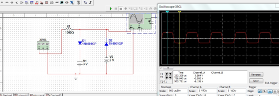
Calculate vour in Figure 6.2, with Vin- 10 Vpp with a frequency of 1 kHz, R 100 Ω, Di-|N4001, RL= 680 Ω. Also, show a computer simulation. 2. Ri out Vin RL. Figure 6.2
Homework Answers
4.
5. given frequancy F= 1Khz
F=1/2*pi* R* C so given R=5.1Kohms substitute R and F values then C=31.2nF.
 2. Vout=8.18V

Add Answer to:
IV, Laboratory Procedure 1. Construct the circuit of Figure 6.1, measure the current value 2. Con...
Prelab a) Look over Section 2-7 of Electronic Devices by Floyd to get a basic understanding...
 Prelab a) Look over Section 2-7 of Electronic Devices by Floyd to get a basic understanding of diode limiters and clampers. b) Design a diode limiter or "clipper circuit which limits input signals to +3 V and -2 V (cf. Floya, Example 2-11). This means that the output signal should not rise above 3 V and should not fall below -2 V. Also calculate the maximum current flowing through each of the diodes. Simulate your clipper in Multisim and compare...
Prelab Preparation: For the RC circuit shown in Figure 1, derive the modeling equation relating the output volta ge...
 Prelab Preparation: For the RC circuit shown in Figure 1, derive the modeling equation relating the output volta ge Vout to the input voltage vin. What is the transfer function? What is the time constant of the system? Vout Figure 1: RC Circuit What is the analytical step response solution in terms of vin, Rand C? For assumed values of R 1 K, and C 6.8 uF, perform a simulation using Matlab/Simulink assuming an input square wave signal of 5Vpp,...
Laboratory 1: operation amplifier characteristics A. Objectives: 1. To study the basic characteri...
 thanks
Laboratory 1: operation amplifier characteristics A. Objectives: 1. To study the basic characteristics of an operational amplifier 2. To study the bias circuit of an operational amplifier B. Apparatus: 1. DC Power supply 2. Experimental board and corresponding components 3. Electronic calculator (prepared by students) 4. Digital camera (prepared by students for photo taking of the experimental results) 5. Laptop computer with the software PicoScope 6 and Microsoft Word installed. 6. PicoScope PC Oscilloscope and its accessories. 7. Multimeter...
thanks
Laboratory 1: operation amplifier characteristics A. Objectives: 1. To study the basic characteristics of an operational amplifier 2. To study the bias circuit of an operational amplifier B. Apparatus: 1. DC Power supply 2. Experimental board and corresponding components 3. Electronic calculator (prepared by students) 4. Digital camera (prepared by students for photo taking of the experimental results) 5. Laptop computer with the software PicoScope 6 and Microsoft Word installed. 6. PicoScope PC Oscilloscope and its accessories. 7. Multimeter...
Experiment and Procedure CIRCUIT 1 10 kOhm 10 kOhm Vin) = 10kOhm 10kOhm V(out) FIGURE 10....
 Experiment and Procedure CIRCUIT 1 10 kOhm 10 kOhm Vin) = 10kOhm 10kOhm V(out) FIGURE 10. PROPORTIONALITY AND LINEARITY 1. Measure and verify all the individual 10 KA resistors shown in Figure 10, then build the given circuit 2. Vary the power supply from OV to 20V in 2V increments. Measure the corresponding output voltages for each input. 3. Calculate the corresponding proportionality constant that relates the output and input voltages. Use the equation: K = 4. Tabularize and plot...
Part I: Inverting Amplifier Procedure: 1. Build the circuit model for inverting amplifier in PSpice with...
 Part I: Inverting Amplifier Procedure: 1. Build the circuit model for inverting amplifier in PSpice with the following parameters: Ri = 5 k 2, R2 = 20 ks2, V+ = 10 V, V-=-10 V. 2. Hand calculates the theoretical closed loop gain Vout/Vin of the circuit model. 3. Generate a triangular waveform for Vin with the amplitude of 1 V and the period of 1 ms. 4. Run simulation. a. Set circuit model parameters. i.e., for voltage source: click VPWL...
Laboratory 2: Transistor circuit characteristics A. Objectives: 1. To study the basic characteris...
 Laboratory 2: Transistor circuit characteristics A. Objectives: 1. To study the basic characteristics of a transistor circuit. 2. To study the bias circuit of a transistor circuit. B. Apparatus: 1. DC Power supply 2. Experimental boards and corresponding components 3. Electronic calculator (prepared by students) 4. Digital camera (prepared by students for photo taking of the experimental results) 5. Laptop computer with the software PicoScope 6 and Microsoft Word installed. 6. PicoScope PC Oscilloscope and its accessories. 7. Digital multi-meter....
In Multisim, rewire your opamp circuit so that it matches the circuit in Figure 2 U1-....
 In Multisim, rewire your opamp circuit so that it matches the circuit in Figure 2 U1-. V4 1kn 0.707 Vrms z OPAMP 3T BASIC R1 0o Figure 2 10. Perform a transient analysis on the circuit. Plot both the input signal (node 3 in Figure 1), and the output (node 1 in Figure 1) on the same graph. Set the time start and end time of the plot to start at zero and run for approximately two cycles of the...
1) For the bridge opamp circuit in the figure, find the total voltage gain expression Vo/Vin...
 1) For the bridge opamp circuit in the figure, find the total voltage gain expression Vo/Vin when the opamps are not saturated. (20p) When Vin (4th) (2001Tt) signal is applied to the input and R1 = R4 = 10K, R2 = R3 = 20K resistance values are selected, draw a single period of the Vo output signal by specifying its time and amplitude values. R2 +12V R1 Vin 1-12V RL Vo +12V -12V WW R3 R4
1. Find the transfer function Voda)/Vin(a) for the circuit shown in Figure 1 of the lab (where co...
 Please answer number 1
1. Find the transfer function Voda)/Vin(a) for the circuit shown in Figure 1 of the lab (where complex frequency variable s jo can be substituted for ease of analysis.) Calculate values for R and C such that the phase shift between the output and input is zero for an input frequency of 10kHz. What is the amplitude ratio (gain) of the output to the input at this frequency. 2. The RC network in figure 3 of...
Please answer number 1
1. Find the transfer function Voda)/Vin(a) for the circuit shown in Figure 1 of the lab (where complex frequency variable s jo can be substituted for ease of analysis.) Calculate values for R and C such that the phase shift between the output and input is zero for an input frequency of 10kHz. What is the amplitude ratio (gain) of the output to the input at this frequency. 2. The RC network in figure 3 of...
Title: Combinational Circuit Design and Simulation Objectives: a. b. c. Design combinational circuit Verify design with...
 Title: Combinational Circuit Design and Simulation Objectives: a. b. c. Design combinational circuit Verify design with simulation Verify design with laboratory test data Materials Needed IBM Compatible computer, PSpice software, IC Chips (as needed), Data Switches, 4702 (1), LED (1). Pre-Lab: Problem Statement The four parameters in a chemical process control system to be monitored are temperature (T), pressure (P), flow (F), and level (L) of the fluid. The parameters are monitored by sensor circuits that produce a High logic...
 Prelab a) Look over Section 2-7 of Electronic Devices by Floyd to get a basic understanding of diode limiters and clampers. b) Design a diode limiter or "clipper circuit which limits input signals to +3 V and -2 V (cf. Floya, Example 2-11). This means that the output signal should not rise above 3 V and should not fall below -2 V. Also calculate the maximum current flowing through each of the diodes. Simulate your clipper in Multisim and compare...
 Prelab Preparation: For the RC circuit shown in Figure 1, derive the modeling equation relating the output volta ge Vout to the input voltage vin. What is the transfer function? What is the time constant of the system? Vout Figure 1: RC Circuit What is the analytical step response solution in terms of vin, Rand C? For assumed values of R 1 K, and C 6.8 uF, perform a simulation using Matlab/Simulink assuming an input square wave signal of 5Vpp,...
 thanks
Laboratory 1: operation amplifier characteristics A. Objectives: 1. To study the basic characteristics of an operational amplifier 2. To study the bias circuit of an operational amplifier B. Apparatus: 1. DC Power supply 2. Experimental board and corresponding components 3. Electronic calculator (prepared by students) 4. Digital camera (prepared by students for photo taking of the experimental results) 5. Laptop computer with the software PicoScope 6 and Microsoft Word installed. 6. PicoScope PC Oscilloscope and its accessories. 7. Multimeter...
thanks
Laboratory 1: operation amplifier characteristics A. Objectives: 1. To study the basic characteristics of an operational amplifier 2. To study the bias circuit of an operational amplifier B. Apparatus: 1. DC Power supply 2. Experimental board and corresponding components 3. Electronic calculator (prepared by students) 4. Digital camera (prepared by students for photo taking of the experimental results) 5. Laptop computer with the software PicoScope 6 and Microsoft Word installed. 6. PicoScope PC Oscilloscope and its accessories. 7. Multimeter...
 Experiment and Procedure CIRCUIT 1 10 kOhm 10 kOhm Vin) = 10kOhm 10kOhm V(out) FIGURE 10. PROPORTIONALITY AND LINEARITY 1. Measure and verify all the individual 10 KA resistors shown in Figure 10, then build the given circuit 2. Vary the power supply from OV to 20V in 2V increments. Measure the corresponding output voltages for each input. 3. Calculate the corresponding proportionality constant that relates the output and input voltages. Use the equation: K = 4. Tabularize and plot...
 Part I: Inverting Amplifier Procedure: 1. Build the circuit model for inverting amplifier in PSpice with the following parameters: Ri = 5 k 2, R2 = 20 ks2, V+ = 10 V, V-=-10 V. 2. Hand calculates the theoretical closed loop gain Vout/Vin of the circuit model. 3. Generate a triangular waveform for Vin with the amplitude of 1 V and the period of 1 ms. 4. Run simulation. a. Set circuit model parameters. i.e., for voltage source: click VPWL...
 Laboratory 2: Transistor circuit characteristics A. Objectives: 1. To study the basic characteristics of a transistor circuit. 2. To study the bias circuit of a transistor circuit. B. Apparatus: 1. DC Power supply 2. Experimental boards and corresponding components 3. Electronic calculator (prepared by students) 4. Digital camera (prepared by students for photo taking of the experimental results) 5. Laptop computer with the software PicoScope 6 and Microsoft Word installed. 6. PicoScope PC Oscilloscope and its accessories. 7. Digital multi-meter....
 In Multisim, rewire your opamp circuit so that it matches the circuit in Figure 2 U1-. V4 1kn 0.707 Vrms z OPAMP 3T BASIC R1 0o Figure 2 10. Perform a transient analysis on the circuit. Plot both the input signal (node 3 in Figure 1), and the output (node 1 in Figure 1) on the same graph. Set the time start and end time of the plot to start at zero and run for approximately two cycles of the...
 1) For the bridge opamp circuit in the figure, find the total voltage gain expression Vo/Vin when the opamps are not saturated. (20p) When Vin (4th) (2001Tt) signal is applied to the input and R1 = R4 = 10K, R2 = R3 = 20K resistance values are selected, draw a single period of the Vo output signal by specifying its time and amplitude values. R2 +12V R1 Vin 1-12V RL Vo +12V -12V WW R3 R4
 Please answer number 1
1. Find the transfer function Voda)/Vin(a) for the circuit shown in Figure 1 of the lab (where complex frequency variable s jo can be substituted for ease of analysis.) Calculate values for R and C such that the phase shift between the output and input is zero for an input frequency of 10kHz. What is the amplitude ratio (gain) of the output to the input at this frequency. 2. The RC network in figure 3 of...
Please answer number 1
1. Find the transfer function Voda)/Vin(a) for the circuit shown in Figure 1 of the lab (where complex frequency variable s jo can be substituted for ease of analysis.) Calculate values for R and C such that the phase shift between the output and input is zero for an input frequency of 10kHz. What is the amplitude ratio (gain) of the output to the input at this frequency. 2. The RC network in figure 3 of...
 Title: Combinational Circuit Design and Simulation Objectives: a. b. c. Design combinational circuit Verify design with simulation Verify design with laboratory test data Materials Needed IBM Compatible computer, PSpice software, IC Chips (as needed), Data Switches, 4702 (1), LED (1). Pre-Lab: Problem Statement The four parameters in a chemical process control system to be monitored are temperature (T), pressure (P), flow (F), and level (L) of the fluid. The parameters are monitored by sensor circuits that produce a High logic...
Most questions answered within 3 hours.
-
A researcher in the field of educational psychology obtains a
random sample of 49 fourth grade...
asked 18 minutes ago -
A
liter of liquid soap concentrate sells for 7.2 Yuan in China.
Determine the total volume...
asked 4 minutes ago -
A
person with polycythemia vera ( excess production of red blood
cells) receives radioactive phosphorus-32. Why...
asked 5 minutes ago -
Regression Analysis
Y = Price in $’s for Tracfone service plan
X1 = No. of minutes...
asked 21 minutes ago -
Various computers and operating systems in the past have used
separate instruction and data spaces, allowing...
asked 9 minutes ago -
You have a series of simple polarisers that you can orient as
you choose in succession...
asked 16 minutes ago -
This is a c++ class utilizing class templates
and linked lists. I need to implement the...
asked 23 minutes ago -
How is the Irish banking system different from the rest of
European banks and how does...
asked 24 minutes ago -
Calculate ΔGo for the reaction of ammonia with
oxygen:
4NH3 (g) + 3 O2 (g)...
asked 26 minutes ago -
How do I go from one concentration of cells to another?
In this case, I have...
asked 27 minutes ago -
Old Faithful geyser in Yellowstone Park shoots water hourly to a
height of 49.2 m. With...
asked 40 minutes ago -
What is the difference between Eddy Currents and Induced
Currents? Are they same if yes, how...
asked 43 minutes ago