The circuit
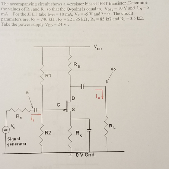
The accompanying circuit shows a 4-resistor biased JFET transistor Determine the values of Rp and Rs so that the Q-point is equal to, VDs 10 V and IDa 5 mA . For the JFET take IDs,-10 mA, VP--5 V and-0. The circuit parameters are, R1 740 ks, R2 221.85 k2, Rs 85 k2 and RL 3.5 k2. Take the power supply VDD 24 V R1 Vi ac R2 Signal generator
Homework Answers

Add Answer to:
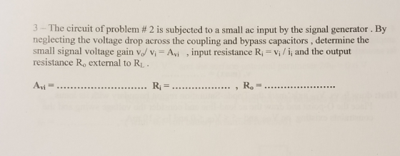
The circuit 3-The circuit of problem # 2 is subjected to a small ac input by the signal generator. By neglecting the voltage drop across the coupling and bypass capacitors, determine the small signa...
please help 2 - The companying circuit shows a 3-resistor biased JFET to be used as...
 please help
2 - The companying circuit shows a 3-resistor biased JFET to be used as a small signal dc amplifier Determine the values of Rp and Rs so that the transistor will meet a point equal to, Vns 8 V and Ips- 2.25 mA .For the JFET take Ipss-4 mA, Vp-4 V and 1- 0 and V coupling and bypass capacitors, determine the small signal voltage gain Vo Vi - Avi which includes RL , input resistance Ri-y /...
please help
2 - The companying circuit shows a 3-resistor biased JFET to be used as a small signal dc amplifier Determine the values of Rp and Rs so that the transistor will meet a point equal to, Vns 8 V and Ips- 2.25 mA .For the JFET take Ipss-4 mA, Vp-4 V and 1- 0 and V coupling and bypass capacitors, determine the small signal voltage gain Vo Vi - Avi which includes RL , input resistance Ri-y /...
#4 The accompanying circuit shows a 4-resistor biased JFET transistor Determine the values of Rp and Rs so that the Q-point is equal to, VDsq 10 V and IDg 5 mA . For the JFET take IDss = 10 mA...
 #4
The accompanying circuit shows a 4-resistor biased JFET transistor Determine the values of Rp and Rs so that the Q-point is equal to, VDsq 10 V and IDg 5 mA . For the JFET take IDss = 10 mA, VP =-5 V and λ 0 . The circuit parameters are, R1-740 k, R2-22 1.85 ka, Rs-85 ㏀ and RL-3.5 ㏀. Take the power supply VDD 24 V 2- Vo R1 Vi R2 Signal generator 4-In reference to the circuit...
#4
The accompanying circuit shows a 4-resistor biased JFET transistor Determine the values of Rp and Rs so that the Q-point is equal to, VDsq 10 V and IDg 5 mA . For the JFET take IDss = 10 mA, VP =-5 V and λ 0 . The circuit parameters are, R1-740 k, R2-22 1.85 ka, Rs-85 ㏀ and RL-3.5 ㏀. Take the power supply VDD 24 V 2- Vo R1 Vi R2 Signal generator 4-In reference to the circuit...
3. Design a n-channel JFET C-S amplifier circuit for the following specifications Voltage Gain input resistance...
 3. Design a n-channel JFET C-S amplifier circuit for the following specifications Voltage Gain input resistance Ri-100kΩ Load resistanceR2k2 Given supply voltage VDD 20V Αν--10 Rss is fully bypassed The input source resistance Rs 02, Ipss-8mA and Vp4V Assume RD and R1 but must find R2 and RSS using the given specifications. Find the DC Operating Points values (VGs, ID and VDs) Draw the actual circuit and its ac equivalent circuit
Exercise 12.13 Derive expressions for the voltage gain, input resistance, and output resistance of the common-gate...
 Exercise 12.13 Derive expressions for the voltage gain, input resistance, and output resistance of the common-gate amplifier shown in Figure 12.29, assuming that ra is an open circuit Answer The small-signal equivalent circuit is shown in Figure 12.30. A Rin 1/(gm 1/Rs); Ro = Rp. gmR/; +VDD С2 + RL Vo CL R + Vin v(t) -Vss W Ri Rp R 8mVgs Vo Rs Vin + v(t)
Exercise 12.13 Derive expressions for the voltage gain, input resistance, and output resistance...
Exercise 12.13 Derive expressions for the voltage gain, input resistance, and output resistance of the common-gate amplifier shown in Figure 12.29, assuming that ra is an open circuit Answer The small-signal equivalent circuit is shown in Figure 12.30. A Rin 1/(gm 1/Rs); Ro = Rp. gmR/; +VDD С2 + RL Vo CL R + Vin v(t) -Vss W Ri Rp R 8mVgs Vo Rs Vin + v(t)
Exercise 12.13 Derive expressions for the voltage gain, input resistance, and output resistance...
This is a very important assignment of mine please do it correctly I will give you...
 This is a very important assignment of mine please do it
correctly I will give you thumbs up
Problem 1. The transistor in the circuit shown to the
right has parameters VTN = 0.4 V, Kn =
= 0.5 mA / V2, and λ
= 0. The circuit parameters are VDD = 3 V and
Ri = R1||R2 = 300 kΩ.
a)Determine the values of R1, R2, and
RS such that IDQ = 0.25 mA and
VDSQ = 1.5 V....
This is a very important assignment of mine please do it
correctly I will give you thumbs up
Problem 1. The transistor in the circuit shown to the
right has parameters VTN = 0.4 V, Kn =
= 0.5 mA / V2, and λ
= 0. The circuit parameters are VDD = 3 V and
Ri = R1||R2 = 300 kΩ.
a)Determine the values of R1, R2, and
RS such that IDQ = 0.25 mA and
VDSQ = 1.5 V....
C- Amplifier: Consider figure 3. This circuit uses the JFET to amplify the input signal voltage F...
 C- Amplifier: Consider figure 3. This circuit uses the JFET to amplify the input signal voltage First the dc operation must be set. Use equation 1 and your previous data to calculate the value of Vas required to give I-0.5 mA. Determine the source resistance Rs needed to set this bias. Set up the circuit of figure 3 with your calculated value of Rs. Measure Vo and Vs to determine if your operating conditions are correct. Apply an input voltage...
Please answer clearly Question 2 The amplifier shown in Figure 2 has the following parameters: Kn(W/L)-1 mA/V2, V-1 V Determine a) Voltage gain (Vo/vi) b) Input resistance (R) c) Output resistance (R...
 Please answer clearly
Question 2 The amplifier shown in Figure 2 has the following parameters: Kn(W/L)-1 mA/V2, V-1 V Determine a) Voltage gain (Vo/vi) b) Input resistance (R) c) Output resistance (Ro) d) Maximum output voltage swing so as the amplifier stays in saturation mode. Assume VDD-20 V, R1-2.5 ΚΩ, R2-1KQ, R3-0.5 ΚΩ, R4-5 MQ, R5_1ΜΩ. R4 R1 R5 R2 Ro R3
Question 2 The amplifier shown in Figure 2 has the following parameters: Kn(W/L)-1 mA/V2, V-1 V Determine a)...
Please answer clearly
Question 2 The amplifier shown in Figure 2 has the following parameters: Kn(W/L)-1 mA/V2, V-1 V Determine a) Voltage gain (Vo/vi) b) Input resistance (R) c) Output resistance (Ro) d) Maximum output voltage swing so as the amplifier stays in saturation mode. Assume VDD-20 V, R1-2.5 ΚΩ, R2-1KQ, R3-0.5 ΚΩ, R4-5 MQ, R5_1ΜΩ. R4 R1 R5 R2 Ro R3
Question 2 The amplifier shown in Figure 2 has the following parameters: Kn(W/L)-1 mA/V2, V-1 V Determine a)...
4) Consider the MOSFET differential amplifier shown below, with Io-2 mA, and RL- 10 kS2, Rss-100 ...
 4) Consider the MOSFET differential amplifier shown below, with Io-2 mA, and RL- 10 kS2, Rss-100 k2, VDD- +8V and Vss--8V. The NMOS transistors in the circuit are nominally identical, with kn 2 mA/V2, VTn 1.0 V and ro 100 k2. The PMoS transistors in the circuit are nominally identical, with kp 2 mA/V2, [VTpl 1.0 V and ro 100 kΩ M3 M4 0 M1 M2 a) First consider the DC bias point. Assuming that the current mirror requires at...
6. Find Vi in the following circuit if VR2 3 V, I -2 A, RI 100...
 6. Find Vi in the following circuit if VR2 3 V, I -2 A, RI 100 , and R2 50 . Ry VR R.y 7. What is the output voltage (Vo) of the summing op-amp below? 1000 kn 200 k2 50 k2 +5 V 100 k2 -5 V V. out 8. For the operational amplifier circuit depicted below: a. Determine Vout in terms of the resistors: Ri, R2, R3, R4 and I R1 qut R- (current source) for the operational...
4. For the amplifier in the figure below use the parameters in the table: +Vcc Re VBE- 0.7V, Ri- ...
 4. For the amplifier in the figure below use the parameters in the table: +Vcc Re VBE- 0.7V, Ri- 1002, R1-160k2, R2-320k2 R3-200k2, R6-40 k2, Rc-60k2, Vcc- 12V, Ry Do a) Draw the DC equivalent circuit and calculate the Q-point. c) Draw the AC equivalent circuit with the small signal model for the transistor. d) Calculate the voltage gain, Av-Vo/vi. Assume ro infinite. e) Draw the circuit to find the amplifier input resistance (Rin). Calculate Rin f Draw the circuit...
 please help
2 - The companying circuit shows a 3-resistor biased JFET to be used as a small signal dc amplifier Determine the values of Rp and Rs so that the transistor will meet a point equal to, Vns 8 V and Ips- 2.25 mA .For the JFET take Ipss-4 mA, Vp-4 V and 1- 0 and V coupling and bypass capacitors, determine the small signal voltage gain Vo Vi - Avi which includes RL , input resistance Ri-y /...
please help
2 - The companying circuit shows a 3-resistor biased JFET to be used as a small signal dc amplifier Determine the values of Rp and Rs so that the transistor will meet a point equal to, Vns 8 V and Ips- 2.25 mA .For the JFET take Ipss-4 mA, Vp-4 V and 1- 0 and V coupling and bypass capacitors, determine the small signal voltage gain Vo Vi - Avi which includes RL , input resistance Ri-y /...
 #4
The accompanying circuit shows a 4-resistor biased JFET transistor Determine the values of Rp and Rs so that the Q-point is equal to, VDsq 10 V and IDg 5 mA . For the JFET take IDss = 10 mA, VP =-5 V and λ 0 . The circuit parameters are, R1-740 k, R2-22 1.85 ka, Rs-85 ㏀ and RL-3.5 ㏀. Take the power supply VDD 24 V 2- Vo R1 Vi R2 Signal generator 4-In reference to the circuit...
#4
The accompanying circuit shows a 4-resistor biased JFET transistor Determine the values of Rp and Rs so that the Q-point is equal to, VDsq 10 V and IDg 5 mA . For the JFET take IDss = 10 mA, VP =-5 V and λ 0 . The circuit parameters are, R1-740 k, R2-22 1.85 ka, Rs-85 ㏀ and RL-3.5 ㏀. Take the power supply VDD 24 V 2- Vo R1 Vi R2 Signal generator 4-In reference to the circuit...
 3. Design a n-channel JFET C-S amplifier circuit for the following specifications Voltage Gain input resistance Ri-100kΩ Load resistanceR2k2 Given supply voltage VDD 20V Αν--10 Rss is fully bypassed The input source resistance Rs 02, Ipss-8mA and Vp4V Assume RD and R1 but must find R2 and RSS using the given specifications. Find the DC Operating Points values (VGs, ID and VDs) Draw the actual circuit and its ac equivalent circuit
 Exercise 12.13 Derive expressions for the voltage gain, input resistance, and output resistance of the common-gate amplifier shown in Figure 12.29, assuming that ra is an open circuit Answer The small-signal equivalent circuit is shown in Figure 12.30. A Rin 1/(gm 1/Rs); Ro = Rp. gmR/; +VDD С2 + RL Vo CL R + Vin v(t) -Vss W Ri Rp R 8mVgs Vo Rs Vin + v(t)
Exercise 12.13 Derive expressions for the voltage gain, input resistance, and output resistance...
Exercise 12.13 Derive expressions for the voltage gain, input resistance, and output resistance of the common-gate amplifier shown in Figure 12.29, assuming that ra is an open circuit Answer The small-signal equivalent circuit is shown in Figure 12.30. A Rin 1/(gm 1/Rs); Ro = Rp. gmR/; +VDD С2 + RL Vo CL R + Vin v(t) -Vss W Ri Rp R 8mVgs Vo Rs Vin + v(t)
Exercise 12.13 Derive expressions for the voltage gain, input resistance, and output resistance...
 This is a very important assignment of mine please do it
correctly I will give you thumbs up
Problem 1. The transistor in the circuit shown to the
right has parameters VTN = 0.4 V, Kn =
= 0.5 mA / V2, and λ
= 0. The circuit parameters are VDD = 3 V and
Ri = R1||R2 = 300 kΩ.
a)Determine the values of R1, R2, and
RS such that IDQ = 0.25 mA and
VDSQ = 1.5 V....
This is a very important assignment of mine please do it
correctly I will give you thumbs up
Problem 1. The transistor in the circuit shown to the
right has parameters VTN = 0.4 V, Kn =
= 0.5 mA / V2, and λ
= 0. The circuit parameters are VDD = 3 V and
Ri = R1||R2 = 300 kΩ.
a)Determine the values of R1, R2, and
RS such that IDQ = 0.25 mA and
VDSQ = 1.5 V....
 C- Amplifier: Consider figure 3. This circuit uses the JFET to amplify the input signal voltage First the dc operation must be set. Use equation 1 and your previous data to calculate the value of Vas required to give I-0.5 mA. Determine the source resistance Rs needed to set this bias. Set up the circuit of figure 3 with your calculated value of Rs. Measure Vo and Vs to determine if your operating conditions are correct. Apply an input voltage...
 Please answer clearly
Question 2 The amplifier shown in Figure 2 has the following parameters: Kn(W/L)-1 mA/V2, V-1 V Determine a) Voltage gain (Vo/vi) b) Input resistance (R) c) Output resistance (Ro) d) Maximum output voltage swing so as the amplifier stays in saturation mode. Assume VDD-20 V, R1-2.5 ΚΩ, R2-1KQ, R3-0.5 ΚΩ, R4-5 MQ, R5_1ΜΩ. R4 R1 R5 R2 Ro R3
Question 2 The amplifier shown in Figure 2 has the following parameters: Kn(W/L)-1 mA/V2, V-1 V Determine a)...
Please answer clearly
Question 2 The amplifier shown in Figure 2 has the following parameters: Kn(W/L)-1 mA/V2, V-1 V Determine a) Voltage gain (Vo/vi) b) Input resistance (R) c) Output resistance (Ro) d) Maximum output voltage swing so as the amplifier stays in saturation mode. Assume VDD-20 V, R1-2.5 ΚΩ, R2-1KQ, R3-0.5 ΚΩ, R4-5 MQ, R5_1ΜΩ. R4 R1 R5 R2 Ro R3
Question 2 The amplifier shown in Figure 2 has the following parameters: Kn(W/L)-1 mA/V2, V-1 V Determine a)...
 4) Consider the MOSFET differential amplifier shown below, with Io-2 mA, and RL- 10 kS2, Rss-100 k2, VDD- +8V and Vss--8V. The NMOS transistors in the circuit are nominally identical, with kn 2 mA/V2, VTn 1.0 V and ro 100 k2. The PMoS transistors in the circuit are nominally identical, with kp 2 mA/V2, [VTpl 1.0 V and ro 100 kΩ M3 M4 0 M1 M2 a) First consider the DC bias point. Assuming that the current mirror requires at...
 6. Find Vi in the following circuit if VR2 3 V, I -2 A, RI 100 , and R2 50 . Ry VR R.y 7. What is the output voltage (Vo) of the summing op-amp below? 1000 kn 200 k2 50 k2 +5 V 100 k2 -5 V V. out 8. For the operational amplifier circuit depicted below: a. Determine Vout in terms of the resistors: Ri, R2, R3, R4 and I R1 qut R- (current source) for the operational...
 4. For the amplifier in the figure below use the parameters in the table: +Vcc Re VBE- 0.7V, Ri- 1002, R1-160k2, R2-320k2 R3-200k2, R6-40 k2, Rc-60k2, Vcc- 12V, Ry Do a) Draw the DC equivalent circuit and calculate the Q-point. c) Draw the AC equivalent circuit with the small signal model for the transistor. d) Calculate the voltage gain, Av-Vo/vi. Assume ro infinite. e) Draw the circuit to find the amplifier input resistance (Rin). Calculate Rin f Draw the circuit...
Most questions answered within 3 hours.
-
A coach uses a new technique to train gymnasts. Seven
gymnasts were randomly selected and their...
asked 44 minutes ago -
While rotating the tires on your car you notice a rock [mass =
0.1 Kg] stuck...
asked 2 hours ago -
Using MARS simulator, write MIPS programs according to
the following scenarios: Receive a positive integer number...
asked 4 hours ago -
An object in front of a concave mirror has a real image that is
11.5 cm...
asked 4 hours ago -
Consider the reaction, C3 H8 + O2 --> CO2 + H2O. How many
moles of O2...
asked 6 hours ago -
You and your opponent both roll a fair die. If you both roll the
same number,...
asked 6 hours ago -
In a study of the accuracy of fast food drive-through orders,
Restaurant A had 257 accurate...
asked 6 hours ago -
Identify and describe in detail the four categories of
institutions that could be included in a...
asked 6 hours ago -
In python
class Customer:
def __init__(self, customer_id, last_name, first_name, phone_number, address):
self._customer_id = int(customer_id)
self._last_name =...
asked 7 hours ago -
What is an example of a limitation in implementing a new
ERP system and how it...
asked 6 hours ago -
In a section of 9.7cm of an artery with a radius of 2.6mm there
is a...
asked 6 hours ago -
the two carboxylic acid groups of aspartic acid have different
acidities with pKa values of 2.1...
asked 7 hours ago