
Homework Answers


Add Answer to:
4) Consider the MOSFET differential amplifier shown below, with Io-2 mA, and RL- 10 kS2, Rss-100 ...
4. Consider the n-channel E-MOSFET amplifier. RD 470Ω RL 3 MS2 C1 Io(on) = 12 mA C1 R2 2ΜΩ Rsig 2...
 4. Consider the n-channel E-MOSFET amplifier. RD 470Ω RL 3 MS2 C1 Io(on) = 12 mA C1 R2 2ΜΩ Rsig 220Ω a) Determine the DC values ofIp, VGs, and VDs b) Find gm c) Determine AvnL, Ri, and Ro. d) Calculate Av, Avs, and Ai
4. Consider the n-channel E-MOSFET amplifier. RD 470Ω RL 3 MS2 C1 Io(on) = 12 mA C1 R2 2ΜΩ Rsig 220Ω a) Determine the DC values ofIp, VGs, and VDs b) Find gm c) Determine...
4. Consider the n-channel E-MOSFET amplifier. RD 470Ω RL 3 MS2 C1 Io(on) = 12 mA C1 R2 2ΜΩ Rsig 220Ω a) Determine the DC values ofIp, VGs, and VDs b) Find gm c) Determine AvnL, Ri, and Ro. d) Calculate Av, Avs, and Ai
4. Consider the n-channel E-MOSFET amplifier. RD 470Ω RL 3 MS2 C1 Io(on) = 12 mA C1 R2 2ΜΩ Rsig 220Ω a) Determine the DC values ofIp, VGs, and VDs b) Find gm c) Determine...
4. For the amplifier in the figure below use the parameters in the table: +Vcc Re VBE- 0.7V, Ri- ...
 4. For the amplifier in the figure below use the parameters in the table: +Vcc Re VBE- 0.7V, Ri- 1002, R1-160k2, R2-320k2 R3-200k2, R6-40 k2, Rc-60k2, Vcc- 12V, Ry Do a) Draw the DC equivalent circuit and calculate the Q-point. c) Draw the AC equivalent circuit with the small signal model for the transistor. d) Calculate the voltage gain, Av-Vo/vi. Assume ro infinite. e) Draw the circuit to find the amplifier input resistance (Rin). Calculate Rin f Draw the circuit...
For the differential amplifier shown in Figure 6: Assume well-matched transistors and = 100 for all transistors: a) Wh...
 For the differential amplifier shown in Figure 6: Assume
well-matched transistors and = 100 for all transistors:
a) Why it is important to use well-matched transistors in
differential amplifier circuits? What is the potential influence of
mismatched transistors on the performance of the differential
amplifier?
b) Determine the resistor values (R1, R2 and R3) such that the
emitter coupled current IE = 0.5 mA and VC1 = 3 V.
c) Draw the ac equivalent circuit for the single ended...
For the differential amplifier shown in Figure 6: Assume
well-matched transistors and = 100 for all transistors:
a) Why it is important to use well-matched transistors in
differential amplifier circuits? What is the potential influence of
mismatched transistors on the performance of the differential
amplifier?
b) Determine the resistor values (R1, R2 and R3) such that the
emitter coupled current IE = 0.5 mA and VC1 = 3 V.
c) Draw the ac equivalent circuit for the single ended...
4. Consider the BJT cascade amplifier shown below Vcc 18V R1 3.3ko 15uF r Vo RL...
 4. Consider the BJT cascade amplifier shown below Vcc 18V R1 3.3ko 15uF r Vo RL B 150 Rsa 500? 56k? Vi B 150 C1 CE 2.2k? a) Find the DC collector current (approximately the same in both transistors). b) Find the input impedance, output impedance, and no-load voltage gain. c) Find the Av, Avs, and Ai d) Estimate the lower cutoff frequency e) Why does this amplifier have better high-frequency performance thana common-emitter built using the same type of...
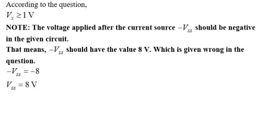
SIM D *8.51 The differential amplifier in Fig. P8.51 utilizes a resistor Rss to establish a 1-mA ...
 Please solve in details and in a clear way.
SIM D *8.51 The differential amplifier in Fig. P8.51 utilizes a resistor Rss to establish a 1-mA de bias current. that this amplifier uses a single 5-V supply and thus the de common-mode voltage Vcoy cannot be zero. Transistors and Q2 have k, W/L = 2.5 mA/V2, V, Note 0.7 V, and λ = 0. in (a) Find the required value of VeM ys: (b) Find the value of Rp that...
Please solve in details and in a clear way.
SIM D *8.51 The differential amplifier in Fig. P8.51 utilizes a resistor Rss to establish a 1-mA de bias current. that this amplifier uses a single 5-V supply and thus the de common-mode voltage Vcoy cannot be zero. Transistors and Q2 have k, W/L = 2.5 mA/V2, V, Note 0.7 V, and λ = 0. in (a) Find the required value of VeM ys: (b) Find the value of Rp that...
Q6. An amplifier circuit using an n-MOSFET is shown in Fig. Q6. The n-MOSFET has the...
 Q6. An amplifier circuit using an n-MOSFET is shown in Fig. Q6. The n-MOSFET has the following parameters: K'-1 mA/V2 and λ-0.02 w. v°' is a small signal AC voltage ource 8V 8V Vout Ra 2.56 mA Fig. Q6 (a) Calculate the DC gate voltage, Va. (b) Assuming that the n-MOSFET is operating in the saturation region and neglecting channel length modulation, calculate the threshold voltage, VrHN, given that the voltage drop across the de current sorce, Inas, has been...
Please answer clearly Question 2 The amplifier shown in Figure 2 has the following parameters: Kn(W/L)-1 mA/V2, V-1 V Determine a) Voltage gain (Vo/vi) b) Input resistance (R) c) Output resistance (R...
 Please answer clearly
Question 2 The amplifier shown in Figure 2 has the following parameters: Kn(W/L)-1 mA/V2, V-1 V Determine a) Voltage gain (Vo/vi) b) Input resistance (R) c) Output resistance (Ro) d) Maximum output voltage swing so as the amplifier stays in saturation mode. Assume VDD-20 V, R1-2.5 ΚΩ, R2-1KQ, R3-0.5 ΚΩ, R4-5 MQ, R5_1ΜΩ. R4 R1 R5 R2 Ro R3
Question 2 The amplifier shown in Figure 2 has the following parameters: Kn(W/L)-1 mA/V2, V-1 V Determine a)...
Please answer clearly
Question 2 The amplifier shown in Figure 2 has the following parameters: Kn(W/L)-1 mA/V2, V-1 V Determine a) Voltage gain (Vo/vi) b) Input resistance (R) c) Output resistance (Ro) d) Maximum output voltage swing so as the amplifier stays in saturation mode. Assume VDD-20 V, R1-2.5 ΚΩ, R2-1KQ, R3-0.5 ΚΩ, R4-5 MQ, R5_1ΜΩ. R4 R1 R5 R2 Ro R3
Question 2 The amplifier shown in Figure 2 has the following parameters: Kn(W/L)-1 mA/V2, V-1 V Determine a)...
5) Consider the Cascode amplifier shown below. For the NMOS transistors, kn 0.2 mA/V2, Vr,-0.5 V,...
 5) Consider the Cascode amplifier shown below. For the NMOS transistors, kn 0.2 mA/V2, Vr,-0.5 V, (W/L)-(W/L)2-5. VDD-GV and IBIAs= 1.0 mA. a) Assuming λ-0 for all transistors, find the required DC gate- source voltages of M1 and M2 (VGsı and VGs2, respectively) BIAS VD out b) Again assuming 0 M2 for all transistors, what is the minimum DC value of VouT for which the amplifier works in high-gain regime? (W/L)2 in M1 For parts c)-f), Assume -0.01 for all...
For the simple differential amplifier shown below, a) Calculate the differential gain, Av , of th...
 For the simple differential amplifier shown below,
a) Calculate the differential gain, Av , of the circuit
b) Calculate the common-mode gain, ACM, of the
circuit and compute CMRR
c) The common-mode gain can be reduced by replacing the resistor
RE, with a constant current source. Design a current
source that is not dependent on Beta linearly to
replace RE, transistors of the same characteristics as
Q1 and Q2, and resistors of your choice
*(Q1, Q2 = 120; ro =...
For the simple differential amplifier shown below,
a) Calculate the differential gain, Av , of the circuit
b) Calculate the common-mode gain, ACM, of the
circuit and compute CMRR
c) The common-mode gain can be reduced by replacing the resistor
RE, with a constant current source. Design a current
source that is not dependent on Beta linearly to
replace RE, transistors of the same characteristics as
Q1 and Q2, and resistors of your choice
*(Q1, Q2 = 120; ro =...
For the differential amplifier shown in Figure (2),
 For the differential amplifier shown in Figure (2),assume \(\mathrm{VCC}=12 \mathrm{~V}, \mathrm{VEE}=-12 \mathrm{~V}, \mathrm{Rc}=2 \mathrm{k} \Omega\), and \(\beta=100\) for all transistors.For the current source circuit (Transistor \(\left.Q_{3}\right): R_{1}=4 k \Omega, R_{2}=4 k \Omega, R_{3}=3 \mathrm{k} \Omega\), and \(r_{0}=100 \mathrm{k} \Omega\).a) In differential amplifier circuits, what do "well-matched transistors" mean?b) Why it is important to use well-matched transistors in differential amplifier circuits?c) What are the operating \(Q\) point values \(\left(I_{c Q}\right.\) and \(\left.V_{C Q}\right)\) for the transistors \(Q_{1}\) and \(Q_{2}\) ?d) Draw...
 4. Consider the n-channel E-MOSFET amplifier. RD 470Ω RL 3 MS2 C1 Io(on) = 12 mA C1 R2 2ΜΩ Rsig 220Ω a) Determine the DC values ofIp, VGs, and VDs b) Find gm c) Determine AvnL, Ri, and Ro. d) Calculate Av, Avs, and Ai
4. Consider the n-channel E-MOSFET amplifier. RD 470Ω RL 3 MS2 C1 Io(on) = 12 mA C1 R2 2ΜΩ Rsig 220Ω a) Determine the DC values ofIp, VGs, and VDs b) Find gm c) Determine...
4. Consider the n-channel E-MOSFET amplifier. RD 470Ω RL 3 MS2 C1 Io(on) = 12 mA C1 R2 2ΜΩ Rsig 220Ω a) Determine the DC values ofIp, VGs, and VDs b) Find gm c) Determine AvnL, Ri, and Ro. d) Calculate Av, Avs, and Ai
4. Consider the n-channel E-MOSFET amplifier. RD 470Ω RL 3 MS2 C1 Io(on) = 12 mA C1 R2 2ΜΩ Rsig 220Ω a) Determine the DC values ofIp, VGs, and VDs b) Find gm c) Determine...
 4. For the amplifier in the figure below use the parameters in the table: +Vcc Re VBE- 0.7V, Ri- 1002, R1-160k2, R2-320k2 R3-200k2, R6-40 k2, Rc-60k2, Vcc- 12V, Ry Do a) Draw the DC equivalent circuit and calculate the Q-point. c) Draw the AC equivalent circuit with the small signal model for the transistor. d) Calculate the voltage gain, Av-Vo/vi. Assume ro infinite. e) Draw the circuit to find the amplifier input resistance (Rin). Calculate Rin f Draw the circuit...
 For the differential amplifier shown in Figure 6: Assume
well-matched transistors and = 100 for all transistors:
a) Why it is important to use well-matched transistors in
differential amplifier circuits? What is the potential influence of
mismatched transistors on the performance of the differential
amplifier?
b) Determine the resistor values (R1, R2 and R3) such that the
emitter coupled current IE = 0.5 mA and VC1 = 3 V.
c) Draw the ac equivalent circuit for the single ended...
For the differential amplifier shown in Figure 6: Assume
well-matched transistors and = 100 for all transistors:
a) Why it is important to use well-matched transistors in
differential amplifier circuits? What is the potential influence of
mismatched transistors on the performance of the differential
amplifier?
b) Determine the resistor values (R1, R2 and R3) such that the
emitter coupled current IE = 0.5 mA and VC1 = 3 V.
c) Draw the ac equivalent circuit for the single ended...
 4. Consider the BJT cascade amplifier shown below Vcc 18V R1 3.3ko 15uF r Vo RL B 150 Rsa 500? 56k? Vi B 150 C1 CE 2.2k? a) Find the DC collector current (approximately the same in both transistors). b) Find the input impedance, output impedance, and no-load voltage gain. c) Find the Av, Avs, and Ai d) Estimate the lower cutoff frequency e) Why does this amplifier have better high-frequency performance thana common-emitter built using the same type of...
 Please solve in details and in a clear way.
SIM D *8.51 The differential amplifier in Fig. P8.51 utilizes a resistor Rss to establish a 1-mA de bias current. that this amplifier uses a single 5-V supply and thus the de common-mode voltage Vcoy cannot be zero. Transistors and Q2 have k, W/L = 2.5 mA/V2, V, Note 0.7 V, and λ = 0. in (a) Find the required value of VeM ys: (b) Find the value of Rp that...
Please solve in details and in a clear way.
SIM D *8.51 The differential amplifier in Fig. P8.51 utilizes a resistor Rss to establish a 1-mA de bias current. that this amplifier uses a single 5-V supply and thus the de common-mode voltage Vcoy cannot be zero. Transistors and Q2 have k, W/L = 2.5 mA/V2, V, Note 0.7 V, and λ = 0. in (a) Find the required value of VeM ys: (b) Find the value of Rp that...
 Q6. An amplifier circuit using an n-MOSFET is shown in Fig. Q6. The n-MOSFET has the following parameters: K'-1 mA/V2 and λ-0.02 w. v°' is a small signal AC voltage ource 8V 8V Vout Ra 2.56 mA Fig. Q6 (a) Calculate the DC gate voltage, Va. (b) Assuming that the n-MOSFET is operating in the saturation region and neglecting channel length modulation, calculate the threshold voltage, VrHN, given that the voltage drop across the de current sorce, Inas, has been...
 Please answer clearly
Question 2 The amplifier shown in Figure 2 has the following parameters: Kn(W/L)-1 mA/V2, V-1 V Determine a) Voltage gain (Vo/vi) b) Input resistance (R) c) Output resistance (Ro) d) Maximum output voltage swing so as the amplifier stays in saturation mode. Assume VDD-20 V, R1-2.5 ΚΩ, R2-1KQ, R3-0.5 ΚΩ, R4-5 MQ, R5_1ΜΩ. R4 R1 R5 R2 Ro R3
Question 2 The amplifier shown in Figure 2 has the following parameters: Kn(W/L)-1 mA/V2, V-1 V Determine a)...
Please answer clearly
Question 2 The amplifier shown in Figure 2 has the following parameters: Kn(W/L)-1 mA/V2, V-1 V Determine a) Voltage gain (Vo/vi) b) Input resistance (R) c) Output resistance (Ro) d) Maximum output voltage swing so as the amplifier stays in saturation mode. Assume VDD-20 V, R1-2.5 ΚΩ, R2-1KQ, R3-0.5 ΚΩ, R4-5 MQ, R5_1ΜΩ. R4 R1 R5 R2 Ro R3
Question 2 The amplifier shown in Figure 2 has the following parameters: Kn(W/L)-1 mA/V2, V-1 V Determine a)...
 5) Consider the Cascode amplifier shown below. For the NMOS transistors, kn 0.2 mA/V2, Vr,-0.5 V, (W/L)-(W/L)2-5. VDD-GV and IBIAs= 1.0 mA. a) Assuming λ-0 for all transistors, find the required DC gate- source voltages of M1 and M2 (VGsı and VGs2, respectively) BIAS VD out b) Again assuming 0 M2 for all transistors, what is the minimum DC value of VouT for which the amplifier works in high-gain regime? (W/L)2 in M1 For parts c)-f), Assume -0.01 for all...
 For the simple differential amplifier shown below,
a) Calculate the differential gain, Av , of the circuit
b) Calculate the common-mode gain, ACM, of the
circuit and compute CMRR
c) The common-mode gain can be reduced by replacing the resistor
RE, with a constant current source. Design a current
source that is not dependent on Beta linearly to
replace RE, transistors of the same characteristics as
Q1 and Q2, and resistors of your choice
*(Q1, Q2 = 120; ro =...
For the simple differential amplifier shown below,
a) Calculate the differential gain, Av , of the circuit
b) Calculate the common-mode gain, ACM, of the
circuit and compute CMRR
c) The common-mode gain can be reduced by replacing the resistor
RE, with a constant current source. Design a current
source that is not dependent on Beta linearly to
replace RE, transistors of the same characteristics as
Q1 and Q2, and resistors of your choice
*(Q1, Q2 = 120; ro =...
Most questions answered within 3 hours.
-
The blues made its way into many kinds of music. Eric Clapton,
The Beatles, and Elvis...
asked 1 hour ago -
8. A wave in a string has a wave function given by: y (x, t) =...
asked 18 minutes ago -
If you’re standing at the bottom of a hill and asked to evaluate
it while being...
asked 2 hours ago -
1. Which region has taken the lead in the world of
e-waste handling?
a) European Union...
asked 2 hours ago -
A 8.15- g bullet from a 9-mm pistol has a velocity of 366.0 m/s.
It strikes...
asked 3 hours ago -
The outstanding bonds of Alpha Extracts have a yield to maturity
of 7.4 percent and a...
asked 3 hours ago -
The Problem: The Case of the Harmonizing Vacations
Your CEO is exploring partnering with a European...
asked 4 hours ago -
A chemical equation is balanced by adding coefficients in front
of some formulas so that the...
asked 4 hours ago -
From the literature (reference your sources): What are the
lattice parameters of calcite and aragonite? Why...
asked 5 hours ago -
Your system is rejecting the question am asking which is
preceded by a case study. It...
asked 5 hours ago -
3. On January 2, 2000, Larry creates a trust with himself as
trustee. Larry as trustee...
asked 5 hours ago -
A member of the volleyball team spikes the ball. During this
process, she changes the velocity...
asked 5 hours ago