
Homework Answers


Add Answer to:
4. Consider the n-channel E-MOSFET amplifier. RD 470Ω RL 3 MS2 C1 Io(on) = 12 mA C1 R2 2ΜΩ Rsig 2...
1.) 120 pointsl The parameters of n-channel enhancement MOSFET in the amplifier circuit below are...
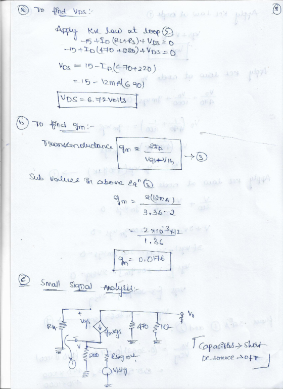
 1.) 120 pointsl The parameters of n-channel enhancement MOSFET in the amplifier circuit below are: 2.042 mA/V2, 1 Val ½ 2.4 V, Kn 150 V a.) Find quiescent values: drain current i, gate-to-source voltage vGs, and drain-to-source voltage vDs b.) Determine AC model parameters: gm and ro c.) Determine amplifier model parameters: Ri, Ro and Avo d) Determine the output voltage Vl across the load RL ǐfv, 1 mYn +VDD GI〈 R ls R Mi RL
1.) 120 pointsl The...
1.) 120 pointsl The parameters of n-channel enhancement MOSFET in the amplifier circuit below are: 2.042 mA/V2, 1 Val ½ 2.4 V, Kn 150 V a.) Find quiescent values: drain current i, gate-to-source voltage vGs, and drain-to-source voltage vDs b.) Determine AC model parameters: gm and ro c.) Determine amplifier model parameters: Ri, Ro and Avo d) Determine the output voltage Vl across the load RL ǐfv, 1 mYn +VDD GI〈 R ls R Mi RL
1.) 120 pointsl The...
1.) [20 points] The parameters of n-channel enhancement MOSFET in the amplifier circuit below are Ve...
 1.) [20 points] The parameters of n-channel enhancement MOSFET in the amplifier circuit below are Ve = 2.4 V, Kn = 2.042 mA/V2, 1VMI = 150 V a.) Find quiescent values: drain current ip, gate-to-source voltage vGs, and drain-to-source voltage vps b.) Determine AC model parameters: gm and ro c.) Determine amplifier model parameters: Ri, Ro and Avo d.) Determine the output voltage vi across the load Rl if vs- 1 mVp SRC
4) Consider the MOSFET differential amplifier shown below, with Io-2 mA, and RL- 10 kS2, Rss-100 ...
 4) Consider the MOSFET differential amplifier shown below, with Io-2 mA, and RL- 10 kS2, Rss-100 k2, VDD- +8V and Vss--8V. The NMOS transistors in the circuit are nominally identical, with kn 2 mA/V2, VTn 1.0 V and ro 100 k2. The PMoS transistors in the circuit are nominally identical, with kp 2 mA/V2, [VTpl 1.0 V and ro 100 kΩ M3 M4 0 M1 M2 a) First consider the DC bias point. Assuming that the current mirror requires at...
1.) 120 points] The parameters of n-channel enhancement MOSFET in the amplifier circuit below are: 2.042...
 1.) 120 points] The parameters of n-channel enhancement MOSFET in the amplifier circuit below are: 2.042 mA/V2, İVMİ V: 2.4 V, Kn 150 V a) Find quiescent values: drain current İD, gate-to-source voltage UGS, and drain-to-source voltage UDS b.) Determine AC model parameters: gm and ro c.) Determine amplifier model parameters: Ri, Ro and Avo d.) Determine the output voltage vi across the load RL f 1 mVp
Design a common-source MOSFET amplifier such that - Rg is a multiple of 10 - Id...
Design a common-source MOSFET amplifier such that - Rg is a multiple of 10 - Id = 0.52 mA - the amplifier input resistance is in the range of mega ohms - | Avo | = 16.7 V/V - RL = 20k - Vsig has a 2kHz frequency - Rsig = 400k, and is the input and the MOSFET has: Vt = 0.8V k = 5 mA/V^2 VA = 80 V Assume capacitors are shorted in the signal circuit and...
Determine the lower and upper cutoff frequency for the network. Sketch the frequency response using bode plot 2. A self-biased n-channel JFET Amplifier with C1(input)-0.01uF C2(bypass)-2uF C3(...
 Determine the lower and upper cutoff frequency for the network.
Sketch the frequency response using bode plot
2. A self-biased n-channel JFET Amplifier with C1(input)-0.01uF C2(bypass)-2uF C3(output)-0.5uF VDD 20V Rsig- 10kQ RG-1M Ω RD-4.7k Q IDSS-8mA VGS(off-AV Cgd-2pF Cgs-4pF Cds-0.5pF Cwo-6pF RL-2.2k Ω Rc rQi=120 0.47uF R, 04uF 0.82Ω R: 2. A self-biased n-channel JFET Amplifier with C1 (input)=001uF C2bypass)-2uF C3(output):0.5UF VDD-20V Rsige 10kΩ RG-1M Ω RD-4.7k Ω IDSS-BmA VGS(off)-4V Cgd-2pF Cds-0.5pF Cwi-5pF RL-2.2k Ω
2. A self-biased n-channel JFET...
Determine the lower and upper cutoff frequency for the network.
Sketch the frequency response using bode plot
2. A self-biased n-channel JFET Amplifier with C1(input)-0.01uF C2(bypass)-2uF C3(output)-0.5uF VDD 20V Rsig- 10kQ RG-1M Ω RD-4.7k Q IDSS-8mA VGS(off-AV Cgd-2pF Cgs-4pF Cds-0.5pF Cwo-6pF RL-2.2k Ω Rc rQi=120 0.47uF R, 04uF 0.82Ω R: 2. A self-biased n-channel JFET Amplifier with C1 (input)=001uF C2bypass)-2uF C3(output):0.5UF VDD-20V Rsige 10kΩ RG-1M Ω RD-4.7k Ω IDSS-BmA VGS(off)-4V Cgd-2pF Cds-0.5pF Cwi-5pF RL-2.2k Ω
2. A self-biased n-channel JFET...
5. Consider the n-channel D-MOSFET amplifier circuit. Ipss and Vp vary in the ranges shown due...
 5. Consider the n-channel D-MOSFET amplifier circuit. Ipss and Vp vary in the ranges shown due to manufacturing variations VDD 12V 5 MS2 330 2 10 HF C1 sig 100 2 0.1 uF RL 1 kS2 10mA s lpss 12 mA -2.5V Vp s-1.5V s GS 1 ΜΩ 250Ω 22 uF Find the resulting variations in Id, gm, and Av. (Hint: you can consider four cases, which make use of the extreme values of Ioss and Vp. This can be...
II) The characteristics of the MOSFET in figure la are shown in figure 1b. Use the characteristic...
 II) The characteristics of the MOSFET in figure la are shown in figure 1b. Use the characteristics in figure 1b, not the equations in your textbook, to answer the following A) From figure lb estimate gm and ro for the FET in the saturation region. Include calculations or an explanation with your answer B Find the values for Re Rd. VDD and VGG so that zin- 100k, zout 5k, L 2 mA and Vds-5 C) Find the GAIN-vo/vi 2oUT Rg...
QUESTION (1) Transistor Mi in this common base amplifier circuit has the following characteristics: +Vc VTH...
 QUESTION (1) Transistor Mi in this common base amplifier circuit has the following characteristics: +Vc VTH =1 V Rp R, C. K 1 mA/V2 2 0.1 R Given: Vcc 2 mA, 10 V, lbias Ct C2 0, 5 k2, RD 2 k2 RI 10 k, R2 R (12 points) a) Determine the small signal gain, vo/Vin. (4 points) b) Determine the input resistance, Rin. (4 points) c) Determine the output resistance, Ro. Useful formulae: for n-channel MOSFET triode region =...
2. (25) You have been given an N-channel enhancement mode MOSFET to be used in the...
 2. (25) You have been given an N-channel enhancement mode MOSFET to be used in the next circuits. The NMOS has the characteristics of Ky = 1.0 mA/V,20, and Vin =1.0 V. A graph o current-voltage characteristics is shown on the next page of the test. (a) Determine resistor values (R. R. Ro Rs) so that Ipo = 4 mA and lose Let Ri= R/ || R 100 K and Vas Vs. Vpp = 12 V. VID = ID. RD"...
 1.) 120 pointsl The parameters of n-channel enhancement MOSFET in the amplifier circuit below are: 2.042 mA/V2, 1 Val ½ 2.4 V, Kn 150 V a.) Find quiescent values: drain current i, gate-to-source voltage vGs, and drain-to-source voltage vDs b.) Determine AC model parameters: gm and ro c.) Determine amplifier model parameters: Ri, Ro and Avo d) Determine the output voltage Vl across the load RL ǐfv, 1 mYn +VDD GI〈 R ls R Mi RL
1.) 120 pointsl The...
1.) 120 pointsl The parameters of n-channel enhancement MOSFET in the amplifier circuit below are: 2.042 mA/V2, 1 Val ½ 2.4 V, Kn 150 V a.) Find quiescent values: drain current i, gate-to-source voltage vGs, and drain-to-source voltage vDs b.) Determine AC model parameters: gm and ro c.) Determine amplifier model parameters: Ri, Ro and Avo d) Determine the output voltage Vl across the load RL ǐfv, 1 mYn +VDD GI〈 R ls R Mi RL
1.) 120 pointsl The...
 1.) [20 points] The parameters of n-channel enhancement MOSFET in the amplifier circuit below are Ve = 2.4 V, Kn = 2.042 mA/V2, 1VMI = 150 V a.) Find quiescent values: drain current ip, gate-to-source voltage vGs, and drain-to-source voltage vps b.) Determine AC model parameters: gm and ro c.) Determine amplifier model parameters: Ri, Ro and Avo d.) Determine the output voltage vi across the load Rl if vs- 1 mVp SRC
 4) Consider the MOSFET differential amplifier shown below, with Io-2 mA, and RL- 10 kS2, Rss-100 k2, VDD- +8V and Vss--8V. The NMOS transistors in the circuit are nominally identical, with kn 2 mA/V2, VTn 1.0 V and ro 100 k2. The PMoS transistors in the circuit are nominally identical, with kp 2 mA/V2, [VTpl 1.0 V and ro 100 kΩ M3 M4 0 M1 M2 a) First consider the DC bias point. Assuming that the current mirror requires at...
 1.) 120 points] The parameters of n-channel enhancement MOSFET in the amplifier circuit below are: 2.042 mA/V2, İVMİ V: 2.4 V, Kn 150 V a) Find quiescent values: drain current İD, gate-to-source voltage UGS, and drain-to-source voltage UDS b.) Determine AC model parameters: gm and ro c.) Determine amplifier model parameters: Ri, Ro and Avo d.) Determine the output voltage vi across the load RL f 1 mVp
 Determine the lower and upper cutoff frequency for the network.
Sketch the frequency response using bode plot
2. A self-biased n-channel JFET Amplifier with C1(input)-0.01uF C2(bypass)-2uF C3(output)-0.5uF VDD 20V Rsig- 10kQ RG-1M Ω RD-4.7k Q IDSS-8mA VGS(off-AV Cgd-2pF Cgs-4pF Cds-0.5pF Cwo-6pF RL-2.2k Ω Rc rQi=120 0.47uF R, 04uF 0.82Ω R: 2. A self-biased n-channel JFET Amplifier with C1 (input)=001uF C2bypass)-2uF C3(output):0.5UF VDD-20V Rsige 10kΩ RG-1M Ω RD-4.7k Ω IDSS-BmA VGS(off)-4V Cgd-2pF Cds-0.5pF Cwi-5pF RL-2.2k Ω
2. A self-biased n-channel JFET...
Determine the lower and upper cutoff frequency for the network.
Sketch the frequency response using bode plot
2. A self-biased n-channel JFET Amplifier with C1(input)-0.01uF C2(bypass)-2uF C3(output)-0.5uF VDD 20V Rsig- 10kQ RG-1M Ω RD-4.7k Q IDSS-8mA VGS(off-AV Cgd-2pF Cgs-4pF Cds-0.5pF Cwo-6pF RL-2.2k Ω Rc rQi=120 0.47uF R, 04uF 0.82Ω R: 2. A self-biased n-channel JFET Amplifier with C1 (input)=001uF C2bypass)-2uF C3(output):0.5UF VDD-20V Rsige 10kΩ RG-1M Ω RD-4.7k Ω IDSS-BmA VGS(off)-4V Cgd-2pF Cds-0.5pF Cwi-5pF RL-2.2k Ω
2. A self-biased n-channel JFET...
 5. Consider the n-channel D-MOSFET amplifier circuit. Ipss and Vp vary in the ranges shown due to manufacturing variations VDD 12V 5 MS2 330 2 10 HF C1 sig 100 2 0.1 uF RL 1 kS2 10mA s lpss 12 mA -2.5V Vp s-1.5V s GS 1 ΜΩ 250Ω 22 uF Find the resulting variations in Id, gm, and Av. (Hint: you can consider four cases, which make use of the extreme values of Ioss and Vp. This can be...
 II) The characteristics of the MOSFET in figure la are shown in figure 1b. Use the characteristics in figure 1b, not the equations in your textbook, to answer the following A) From figure lb estimate gm and ro for the FET in the saturation region. Include calculations or an explanation with your answer B Find the values for Re Rd. VDD and VGG so that zin- 100k, zout 5k, L 2 mA and Vds-5 C) Find the GAIN-vo/vi 2oUT Rg...
 QUESTION (1) Transistor Mi in this common base amplifier circuit has the following characteristics: +Vc VTH =1 V Rp R, C. K 1 mA/V2 2 0.1 R Given: Vcc 2 mA, 10 V, lbias Ct C2 0, 5 k2, RD 2 k2 RI 10 k, R2 R (12 points) a) Determine the small signal gain, vo/Vin. (4 points) b) Determine the input resistance, Rin. (4 points) c) Determine the output resistance, Ro. Useful formulae: for n-channel MOSFET triode region =...
 2. (25) You have been given an N-channel enhancement mode MOSFET to be used in the next circuits. The NMOS has the characteristics of Ky = 1.0 mA/V,20, and Vin =1.0 V. A graph o current-voltage characteristics is shown on the next page of the test. (a) Determine resistor values (R. R. Ro Rs) so that Ipo = 4 mA and lose Let Ri= R/ || R 100 K and Vas Vs. Vpp = 12 V. VID = ID. RD"...
Most questions answered within 3 hours.
-
(in Java) We wish to insert the following strings into a hash
table: BEN AL SUE...
asked 4 minutes ago -
Group think happens when the members of the group become more
interested in agreeing with each...
asked 3 minutes ago -
how might the HR Scorecard might be used to demonstrate value
creation that aligns with the...
asked 20 minutes ago -
If the racetrack publishes that the odds in favor of a horse
winning a race are...
asked 28 minutes ago -
2.
A particular sample of vinegar has a pH of 2.95.
Part A
If acetic acid...
asked 34 minutes ago -
1a.) A simple random sample of 100 Harvard undergraduates was
given a two-question astronomy test. 13%...
asked 38 minutes ago -
A spider hangs vertically from a thread of negligible mass. In
what situation, the tension in...
asked 40 minutes ago -
is an approach for addressing bottlenecks in a process or
system.
A. Utilization
B. Breakeven Analysis...
asked 1 hour ago -
A 125 g sample of an unknown substance is heated to 93.6 °C and
then dropped...
asked 52 minutes ago -
How is a car horn like an earthquake? How is it different? Which
of the waves...
asked 56 minutes ago -
Currently, GH Co. sells 42,600 handbags annually at an average
price of $149 each. It is...
asked 1 hour ago -
A boy of mass 60 kg and a girl of mass 40 kg are together and...
asked 1 hour ago