
Homework Answers


Add Answer to:
QUESTION (1) Transistor Mi in this common base amplifier circuit has the following characteristics: +Vc VTH...
V.+w Operation in the triode reglon Condition v. e Wov 20 Vos uov os os-V (2) p V, so onl+Pala Characteristics Same rel...
 V.+w Operation in the triode reglon Condition v. e Wov 20 Vos uov os os-V (2) p V, so onl+Pala Characteristics Same relationships as for NMOS trasistos tCharacteristics: a CuGs- V,) ®os- } ip.C Replace .and NA with p,,and Nprespectively. V.V V, and yare negative. 2 wov ps For vos 2( -V) e Conditions for operation in the triode region ip lvi Q1. (10 points) For the following configuration of the given figure below, with the following parameters: VDD= +10...
QUESTION (3) For this circuit, VTH = 1 V (for both transistors Mi and M2) 0.01...
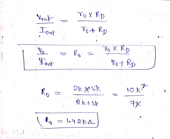
 QUESTION (3) For this circuit, VTH = 1 V (for both transistors Mi and M2) 0.01 V Re C = 2 mA/V2 M, C, Ibeas = 2 mA a) Determine the gain volv,. b) Determine the input and output resistance, Rin and Ro c) (10 points) 5 points) What is maximum peak to peak input voltage that can be -VEE applied while still keeping Mi operating in the saturation (5 points) region?
Consider an nMOS transistor with VTH = 0.4 V, Kn = 140μA/V2 , length, L =...
Consider an nMOS transistor with VTH = 0.4 V, Kn = 140μA/V2 , length, L = 0.25μm, and width, W = 1.25μm. (a) Given that VGS = 1V, determine the range of values of VDS for which the device is in the saturation region. (b) Given that VGS = 1V, determine the range of values of VDS for which the device is in the triode/linar region. (c) Plot IDS vs VGS for operation in the saturation region. Ignore channel length...
In the circuit shown in Figure P11.11, the MOSFET operates in the active region, for iD...
 In the circuit shown in Figure P11.11, the MOSFET operates in
the active region, for iD = 0.5 mA and vD = 3 V. This
enhancement-type PMOS has VT =−1 V,k = 0.5 mA/V2.
Find
a. RD.
b. The largest allowable value of RD for the MOSFET to remain in
the saturation region.
ip VDS VDD10 V VGS R2 Rp Figure P11.11 ww
ip VDS VDD10 V VGS R2 Rp Figure P11.11 ww
In the circuit shown in Figure P11.11, the MOSFET operates in
the active region, for iD = 0.5 mA and vD = 3 V. This
enhancement-type PMOS has VT =−1 V,k = 0.5 mA/V2.
Find
a. RD.
b. The largest allowable value of RD for the MOSFET to remain in
the saturation region.
ip VDS VDD10 V VGS R2 Rp Figure P11.11 ww
ip VDS VDD10 V VGS R2 Rp Figure P11.11 ww
Please help with the LT SPICE for this nmos transistor analysis problem. I figured out the calcul...
 please help with the LT SPICE for this nmos transistor analysis
problem. I figured out the calculations, I just need help verifying
them with LT SPICE. thank you!
Analyze the following MOSFET circuit for dc bias. Solve for ID, VGs and VDs Use RD-5 kQ, Rs-5 kQ, RG,-1 ΜΩ and RG2-1 MS2. Use a power supply with VDD-| 2 V and K.-I mA/V2 and Vin-1 V. RG RD RG2 Rs Verify the analysis of the circuit of Prob. 5 by...
please help with the LT SPICE for this nmos transistor analysis
problem. I figured out the calculations, I just need help verifying
them with LT SPICE. thank you!
Analyze the following MOSFET circuit for dc bias. Solve for ID, VGs and VDs Use RD-5 kQ, Rs-5 kQ, RG,-1 ΜΩ and RG2-1 MS2. Use a power supply with VDD-| 2 V and K.-I mA/V2 and Vin-1 V. RG RD RG2 Rs Verify the analysis of the circuit of Prob. 5 by...
SIM D 7.98 Design the circuit in Fig. P7.98 so that the transistor operates in saturation...
 SIM D 7.98 Design the circuit in Fig. P7.98 so that the transistor operates in saturation with V, biased 1 V from the edge of the triode region, with 1, = 1 mA and V, = 3 V, for each of the following two devices (use a 10-mA current in the voltage divider): (a) V=1 V and k WIL = 0.5 mA/V2 (b) V=2 V and k WIL = 1.25 mA/V2 For each case, specify the values of V, V,...
An NMOS transistor with parameters VTh=1 V, k’=100 uA/V2 , W = 10 um, and L=1...
An NMOS transistor with parameters VTh=1 V, k’=100 uA/V2 , W = 10 um, and L=1 um has a VGS=2 V. Find the drain current when: a. VDS=0.5 V b. VDS=2 V c. VDS=3 V Answers: a) 374 uA b) 0.5 mA c) 0.5 mA please show your work :)
3. (2 points) For the D-MOSFET circuit shown below, VDD 20 V, R1 1.8 M2, R2...
 3. (2 points) For the D-MOSFET circuit shown below, VDD 20 V, R1 1.8 M2, R2 200 k2, Ro 1.5 k(2, Rs = 470 ?, VGS(OFF)--5 V, and loss 10 mA. a. If the transistor is operating at IDQ = 6.4 mA and VGSQ-_1.0 V, is the MOSFET Solve for Vosa. (Extra credit: 1 point) Determine the operating point graphically (hint: first decide DC load line using two points, then use the similar procedure in the previous problem. b. c....
VOD Ro 1. [Design Problem (1)] N-channel MOSFET (NMOS) operating in "Saturation" region. a. Consider a...
 VOD Ro 1. [Design Problem (1)] N-channel MOSFET (NMOS) operating in "Saturation" region. a. Consider a circuit as shown in Fig 1. b. You will need to design the circuit such that Ip = 1 (mA), VG = 0 [V], and Vp = 5 [V]. (determine values for R1, R2, Rp, and Rs) 1 W ID = 5 unCox (Vgs - Vrh)2 = K (Vgs - VTH)2 c. Use Vpp = 15 [V], Vs = -15 [V], and 2N7000 for...
Solve for VGS, Ip, and Vds for this NMOS transistor circuit. Vpp = +6.0V Rp =...
 Solve for VGS, Ip, and Vds for this NMOS transistor circuit. Vpp = +6.0V Rp = 4.9 kN2 RG1 = 2 M12 Rs = 2.0 ks2 RG2= 1 M 2 RD kn = 10.0 mA/V2 RG1 Vi= 1.0 V RG2 O Vss = -6.0V
 V.+w Operation in the triode reglon Condition v. e Wov 20 Vos uov os os-V (2) p V, so onl+Pala Characteristics Same relationships as for NMOS trasistos tCharacteristics: a CuGs- V,) ®os- } ip.C Replace .and NA with p,,and Nprespectively. V.V V, and yare negative. 2 wov ps For vos 2( -V) e Conditions for operation in the triode region ip lvi Q1. (10 points) For the following configuration of the given figure below, with the following parameters: VDD= +10...
 QUESTION (3) For this circuit, VTH = 1 V (for both transistors Mi and M2) 0.01 V Re C = 2 mA/V2 M, C, Ibeas = 2 mA a) Determine the gain volv,. b) Determine the input and output resistance, Rin and Ro c) (10 points) 5 points) What is maximum peak to peak input voltage that can be -VEE applied while still keeping Mi operating in the saturation (5 points) region?
 In the circuit shown in Figure P11.11, the MOSFET operates in
the active region, for iD = 0.5 mA and vD = 3 V. This
enhancement-type PMOS has VT =−1 V,k = 0.5 mA/V2.
Find
a. RD.
b. The largest allowable value of RD for the MOSFET to remain in
the saturation region.
ip VDS VDD10 V VGS R2 Rp Figure P11.11 ww
ip VDS VDD10 V VGS R2 Rp Figure P11.11 ww
In the circuit shown in Figure P11.11, the MOSFET operates in
the active region, for iD = 0.5 mA and vD = 3 V. This
enhancement-type PMOS has VT =−1 V,k = 0.5 mA/V2.
Find
a. RD.
b. The largest allowable value of RD for the MOSFET to remain in
the saturation region.
ip VDS VDD10 V VGS R2 Rp Figure P11.11 ww
ip VDS VDD10 V VGS R2 Rp Figure P11.11 ww
 please help with the LT SPICE for this nmos transistor analysis
problem. I figured out the calculations, I just need help verifying
them with LT SPICE. thank you!
Analyze the following MOSFET circuit for dc bias. Solve for ID, VGs and VDs Use RD-5 kQ, Rs-5 kQ, RG,-1 ΜΩ and RG2-1 MS2. Use a power supply with VDD-| 2 V and K.-I mA/V2 and Vin-1 V. RG RD RG2 Rs Verify the analysis of the circuit of Prob. 5 by...
please help with the LT SPICE for this nmos transistor analysis
problem. I figured out the calculations, I just need help verifying
them with LT SPICE. thank you!
Analyze the following MOSFET circuit for dc bias. Solve for ID, VGs and VDs Use RD-5 kQ, Rs-5 kQ, RG,-1 ΜΩ and RG2-1 MS2. Use a power supply with VDD-| 2 V and K.-I mA/V2 and Vin-1 V. RG RD RG2 Rs Verify the analysis of the circuit of Prob. 5 by...
 SIM D 7.98 Design the circuit in Fig. P7.98 so that the transistor operates in saturation with V, biased 1 V from the edge of the triode region, with 1, = 1 mA and V, = 3 V, for each of the following two devices (use a 10-mA current in the voltage divider): (a) V=1 V and k WIL = 0.5 mA/V2 (b) V=2 V and k WIL = 1.25 mA/V2 For each case, specify the values of V, V,...
 3. (2 points) For the D-MOSFET circuit shown below, VDD 20 V, R1 1.8 M2, R2 200 k2, Ro 1.5 k(2, Rs = 470 ?, VGS(OFF)--5 V, and loss 10 mA. a. If the transistor is operating at IDQ = 6.4 mA and VGSQ-_1.0 V, is the MOSFET Solve for Vosa. (Extra credit: 1 point) Determine the operating point graphically (hint: first decide DC load line using two points, then use the similar procedure in the previous problem. b. c....
 VOD Ro 1. [Design Problem (1)] N-channel MOSFET (NMOS) operating in "Saturation" region. a. Consider a circuit as shown in Fig 1. b. You will need to design the circuit such that Ip = 1 (mA), VG = 0 [V], and Vp = 5 [V]. (determine values for R1, R2, Rp, and Rs) 1 W ID = 5 unCox (Vgs - Vrh)2 = K (Vgs - VTH)2 c. Use Vpp = 15 [V], Vs = -15 [V], and 2N7000 for...
 Solve for VGS, Ip, and Vds for this NMOS transistor circuit. Vpp = +6.0V Rp = 4.9 kN2 RG1 = 2 M12 Rs = 2.0 ks2 RG2= 1 M 2 RD kn = 10.0 mA/V2 RG1 Vi= 1.0 V RG2 O Vss = -6.0V
Most questions answered within 3 hours.
-
You and your opponent both roll a fair die. If you both roll the
same number,...
asked 6 minutes ago -
In a study of the accuracy of fast food drive-through orders,
Restaurant A had 257 accurate...
asked 6 minutes ago -
Identify and describe in detail the four categories of
institutions that could be included in a...
asked 12 minutes ago -
In python
class Customer:
def __init__(self, customer_id, last_name, first_name, phone_number, address):
self._customer_id = int(customer_id)
self._last_name =...
asked 19 minutes ago -
What is an example of a limitation in implementing a new
ERP system and how it...
asked 14 minutes ago -
In a section of 9.7cm of an artery with a radius of 2.6mm there
is a...
asked 15 minutes ago -
the two carboxylic acid groups of aspartic acid have different
acidities with pKa values of 2.1...
asked 19 minutes ago -
Would CuCO3 aqueous salt combined with calcium chloride
form a solid precipitate? If so, what would...
asked 18 minutes ago -
How do ECM Solutions assist in embedding a culture of continuous
improvement in an organization? (Project...
asked 39 minutes ago -
Directions
These directions introduce the idea of Essential Questions.
Since this may be a new concept...
asked 41 minutes ago -
1.b. Fiscal policy is said to suffer from ‘crowding out’.
Explain what this means and why...
asked 58 minutes ago -
The equation for the reaction of nitrogen and oxygen to form
nitrogen oxide is written as...
asked 1 hour ago